5
4
3
2
1
A
B
C
D
E
F
G
H
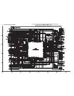
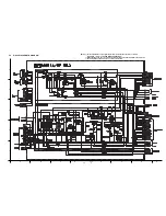
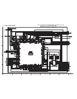
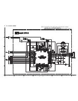
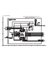
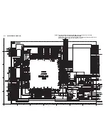
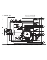
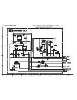
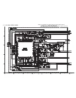
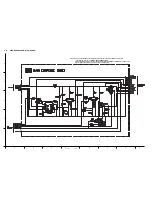
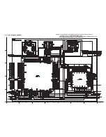
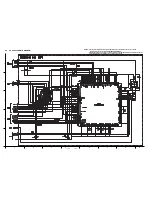
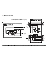
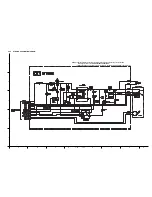
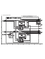
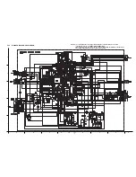
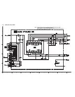
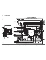
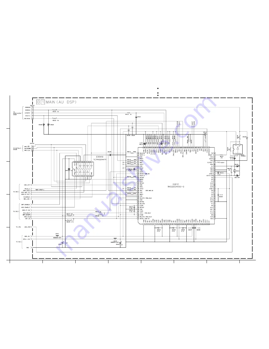
4.17 AU DSP SCHEMATIC DIAGRAM
4-35
4-36
NOTES:
For the destination of each signal and further line connections that are cut off from
this diagram, refer to “4.1 BOARD INTERCONNECTIONS”.
When ordering parts, be sure to order according to the Part Number indicated in the Parts List.
According to the parts which have no values are not used.
Summary of Contents for GR-DVM90U
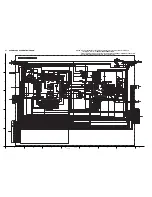
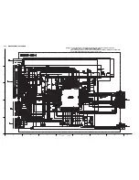
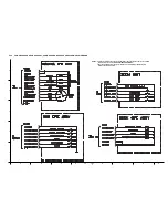
Page 45: ...5 4 3 2 1 A B C D E F G H 4 1 BOARD INTERCONNECTIONS 4 3 4 4 ...
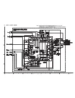
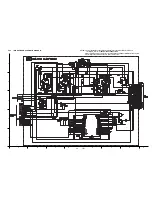
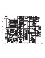
Page 75: ...5 4 3 2 1 A B C D E F G H 4 37 POWER SYSTEM BLOCK DIAGRAM 4 79 4 80 ...
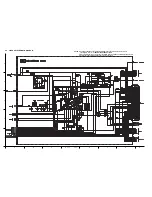
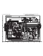
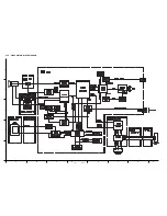
Page 76: ...5 4 3 2 1 A B C D E F G H 4 38 VIDEO SYSTEM BLOCK DIAGRAM 4 81 4 82 ...
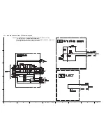
Page 77: ...5 4 3 2 1 A B C D E F G H 4 39 REGULATOR SYSTEM BLOCK DIAGRAM 4 83 4 84 ...

