background image

1-12

1.11

EMERGENCY DISPLAY FUNCTION

This unit has a function for storing the history of the past two
emergencies (EMG) and displaying them on each FDP. With
the status of the VCR and mechanism at the moment an emer-
gency occurred can also be confirmed.

Notes:

The emergency detail display

  1  2  

show the information

on the latest emergency.
It becomes “ – – : – – : – –” when there is no latest emer-
gency record.

When using the Jig RCU, set its custom code to match
the custom code of the VCR.

FDP display   0 : 00 : 

00


Emergency detail display  2

Emergency detail display  1

Emergency content display 
(E:Latest:Previous)

Normal display

*

1: 

*

2 : 

3 4

E: 

**

**

*

5: 

*

6 : 

*

7

Fig. 1-11-1   Jig RCU [PTU94023B]

Note:

For the emergency content, see “1.11.3  Emergency con-
tent description”.

(2) Transmit the code “59” from the Jig RCU again.

The FDP shows the emergency detail information  1  in the
form of “

*

1 : 

*

2 : 

3 4

”.

*

1

: Deck operation mode at the moment of emergency

*

2

: Mechanism operation mode at the moment of emer-

gency


3 –

: Mechanism sensor information at the moment of

emergency

 – 4

:

Mechanism mode position at the moment of emer-
gency

Note:

For the emergency detail information


  1


, see “1.11.4

Emergency detail information


”.

(3) Transmit the code “59” from the Jig RCU once again.

The FDP shows the emergency detail information


2 in the

form of “

*

5

 : 

*

6

 : 

*

7

”.

*

5

: Type of the cassette tape in use


 1 .

*

6

: Winding position of the cassette tape in use

*

7

: Type of the cassette tape in use


 2 (Winding area)

Note:

For the emergency detail information  

, see “1.11.5  Emer-

gency detail information  

2

 ”.

(4) Transmit the code “59” from the Jig RCU once again to re-

set the display.

1.11.2 Clearing the emergency history

(1) Display the emergency history.
(2) Transmit the code “36” from the Jig RCU.
(3) Reset the emergency display.

Example 1     E : 01 : 

03

Previous emergency

Latest emergency

  No emergency record

Example 2

E : – – : 

– –

1.11.1 Displaying the emergency information

(1) Transmit the code “59” from the Jig RCU.

The FDP shows the emergency content in the form of
“E:

**

:

* *

”.

INITIAL MODE

DATA CODE

CUSTOM CODE
43: A

CODE

53: B

CODE

6F: C

CODE

7F: D

CODE

[Data transmitting method]
Depress the “    ” (  3  ) button 
after the data code is set.

Jig RCU

FDP display switching

Summary of Contents for HM-HDS1EU

Page 1: ...hours SEP 40 hours VHS DECK VIDEO AUDIO Signal system PAL type colour signal and CCIR monochrome signal 625 lines 50 fields Recording system DA4 Double Azimuth head helical scan system Format S VHS VHS PAL standard Signal to noise ratio 45 dB Horizontal resolution SP LP 250 lines VHS 400 lines S VHS EP 220 lines VHS 350 lines S VHS Frequency range 70 Hz to 10 000 Hz Normal audio 20 Hz to 20 000 Hz...

Page 2: ... inner package carton only for transport ing an HDD s Do not stack package cartons one upon another 1 2 Handling an HDD in the stand alone status s When handling an HDD on a hard workbench place an antistatic mat rubber sheet or similar object on the hard surface to prevent any impacts occurring between the HDD and bench s Do not stack the HDDs one upon another s Do not knock an HDD with a hard ob...

Page 3: ...m the remote jig for more than 2 seconds 2 The REC LINK button on the HDD VHS DUAL RECORDER blinks indicating that the power supply can be switched ON 3 When the code AE is transmitted again from the remote jig the button stops blinking and its function is canceled Initial mode Data code Custom code 43 A code 52 B code 6F C code 7F D code HDD OK HM HDS1 POWER BS DIGIATL CHANNEL Blinks ASIC_IF MPEG...

Page 4: ... 1 5 EVR Adjustment 3 1 TABLE OF CONTENTS Section Title Page Section Title Page 3 2 SERVO CIRCUIT 3 2 3 2 1 Switching point 3 2 3 2 2 Slow tracking preset 3 2 3 3 VIDEO CIRCUIT 3 2 3 3 1 D A level 3 2 3 3 2 EE Y level 3 3 3 3 3 PB Y level S VHS VHS 3 3 3 3 4 REC color colour level 3 3 3 3 5 Video EQ Frequency response 3 4 3 3 6 AUTO PICTURE initial setting 3 4 3 4 DIGITAL CIRCUIT 3 4 3 4 1 HDD EE ...

Page 5: ...e specified for compli ance with recognized codes pertaining to X ray emission Consequently when servicing these products replace the cath ode ray tubes and other parts with only the specified parts Under no circumstances attempt to modify these circuits Unauthorized modification can increase the high voltage value and cause X ray emission from the cathode ray tube 12 Crimp type wire connector In ...

Page 6: ... between terminals and surrounding metallic parts See table 1 below 4 Leakage current test Confirm specified or lower leakage current between earth ground power cord plug prongs and externally exposed accessible parts RF terminals antenna terminals video and audio input and output terminals microphone jacks earphone jacks etc Measuring Method Power ON Insert load Z between earth ground power cord ...

Page 7: ...hose on the spare parts list 5 Adjustment information for installation Fig 1 1 1 1 2 3 4 5 Step Loc No Fig No Point Note Part name Top cover Bracket COM1 4 S1 3 S2 2 L1 L2 2 S3 1 Front panel assembly COM2 8 L3 CN7507 WR1 CN3011 WR2 Note 1 2 3 4 2 1 3 DISCONNECTION OF CONNECTORS WIRES CONNECTOR FPC CONNECTOR FPC Fig 1 3 1 Fig 1 3 2 Fig 1 3 3 Fig 1 3 4 CONNECTOR FPC Fig 1 3 5 CONNECTOR FPC CONNECTOR...

Page 8: ...y or Regula tor board assembly unhook the several spacers connect ing it with pliers from the top side Note 5 Perform the work by leaving fan motor attached to the rear cover except when replacing the fan motor When attaching the rear cover please be careful with the wiring 1 5 2 Disassembly assembly method COM section Fig COM1 7 S2 5 S2 4 S1 3 S1 6 S2 2 S1 1 S1 1 L1 L2 1 Top cover 8 S3 9 S3 Brack...

Page 9: ...S4 20 S4 14 S4 18 S4 13 S4 12 S4 11 S4 10 S4 23 S4 Display board assembly LED SW board assembly LED board assembly Jack board assembly Eject SW board assembly 3 2 5 CN5325 CN5326 WR8 WR5 Foil side Note 1 WR4 Foil side Note 1 WR6 WR7 CN5321 CN5322 L6 Spacer Note 4 L6 Spacer Note 4 CN5323 4 27 S5 WR3 Supporting tape side Note 1 L4 Spacer Note 4 L5 CN5301 26 S5 ...

Page 10: ...the Main board assembly take care not to damage the sensors on the Main board assembly D3001 LED Q3002 Start sen sor Q3003 End sensor S3002 S cassette switch Fig 1 Fig 2 Fig 3 Procedures for Lowering the Cassette holder assembly As the mechanism of this unit is integrated with the Housing assembly the holder must be lowered and the two screws un screwed when removing the Mechanism assembly Procedu...

Page 11: ...S3 Note 4 4 S3 Note 4 WR11 Foil side Note 2 6 S8 7 S9 2 8 S3 10 S5 9 S3 WR16 Foil side Note 2 CN5322 CN703 WR15 CN2601 CN3014 WR4 Foil side Note 2 WR5 Foil side Note 2 WR14 Foil side Note 2 CN5321 3 Fig V4 11 S3 14 S5 13 S5 12 S5 4 Note When installing the Mechanism assembly secure the screws S8 in the order of a b ...

Page 12: ...ire to the connector be sure to connect it in the correct orientation Note 4 When removing the board assembly take care not to dam age it Fig H1 Fig H2 1 Hard disk drive assembly 2 Hard disk drive 3 Digital board assembly 1 7 HOW TO REMOVE THE MAJOR PARTS HDD section 1 7 1 Disassembly flow chart This flowchart shows the disassembly procedure for the ex terior parts and electrical parts Basically r...

Page 13: ...sembly A 1 2 6 7 3 4 5 B E CN7507 CN3011 CN3014 CN703 CN2601 CN7508 CN7509 CN5322 CN5321 C D CN8801 CN8601 CN8002 Fig 1 8 1 Service position VHS side Table 1 8 1 Installation 1 Stand up the bottom chassis assembly so that the Regu lator side is in the lower position 2 Connect the PATCH CORD to the three FPCs then con nect CN3014 CN7508 and CN7509 3 By connecting a total of two FPCs and wires CN703...

Page 14: ...lator board assembly Table 1 8 3 SYMBOL CONNECTOR WIRE CONNECTIONS PIN No PATCH CORD I II 1 MAIN CN7507 JACK CN7002 10 A I II 2 MAIN CN3011 DISPLAY CN7001 18 B I 3 TERMINAL CN703 DIGITAL CN8601 6 I 4 MAIN CN7508 REGULATOR CN5322 13 C I 5 MAIN CN7509 REGULATOR CN5321 15 D I 6 MAIN CN2601 DIGITAL CN8801 8 I II 7 MAIN CN3014 DIGITAL CN8002 6 E II 8 DIGITAL CN8001 HARD DISK DRIVE 40 II 9 REGULATOR CN5...

Page 15: ...the Pro cedures for Lowering the Cassette holder assembly on page 1 5 of 1 6 HOW TO REMOVE THE MAJOR PARTS VHS section 6 The cassette holder lowers and when the loading has completed the mechanism enters the desired mode VR1401 D A LEVEL ADJ TPGND TP701 D AGC VR701 DV AGC TPGND TP7001 TEST TP106 PB FM TP4001 CTL P TP111 D FF TP2253 A PB FM Hard disk drive HDD CN3011 CN7507 Main board assembly Term...

Page 16: ... CN8001 CN8002 CN8801 CN8601 CN703 CN7506 CN512 CN7508 CN2601 CN3001 CN2001 CN1 CN1 CON1 CN7509 CN3014 6 3 4 9 5 8 1 2 13 14 15 16 11 12 10 A C HEAD DRUM FAN motor B D CN3011 CN7507 7 CN3014 Main board assembly Main board assembly Main board assembly Chassis Absorb the looseness of the wire in the B part Treat the front wires according to the figure DETAIL B Frame Digital board assembly The wire s...

Page 17: ...N5325 FAN MOTOR 2 WIRE 7 WR7 REGULATOR CN5326 HDD 4 WIRE 8 WR8 REGULATOR CN5323 DIGITAL CN8901 9 WIRE 9 WR9 DRUM MOTOR CON1 MAIN CN3001 5 FPC 10 WR10 MAIN CN1 UPPER DRUM 11 FPC 11 WR11 A C HEAD CN1 MAIN CN2001 7 FPC 12 WR12 MAIN CN3014 DIGITAL CN8002 6 FPC 13 WR13 MAIN CN703 DIGITAL CN8601 6 WIRE 14 WR14 MAIN CN2601 DIGITAL CN8801 8 FPC 15 WR15 DIGITAL CN8001 HDD 40 WIRE 16 MAIN CN7506 S SUB CN512...

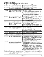
Page 18: ...nism sensor information at the moment of emergency 4 Mechanism mode position at the moment of emer gency Note For the emergency detail information 1 see 1 11 4 Emergency detail information 1 3 Transmit the code 59 from the Jig RCU once again The FDP shows the emergency detail information 2 in the form of 5 6 7 5 Type of the cassette tape in use 1 6 Winding position of the cassette tape in use 7 Ty...

Page 19: ... voltage DRUM CTL V is not supplied to the MDA 4 Power is not supplied to the drum MDA 1 The cassette cannot be ejected due to a failure in the drive mechanism of the housing 2 When the housing load increases during ejection the loading motor is stopped because of lack of headroom in its drive torque Housing load increasing factors Temperature environment low tempera ture etc mechanism wear or fai...

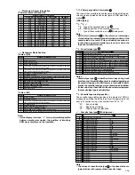
Page 20: ... compression OFF as a result of POWER OFF 16 Mode transition to STOP with pinch roller compression ON as a result of POWER ON 18 Mode transition to PLAY 1A Mode transition to FWD SEARCH 1C Mode transition to REC 1E Mode transition to FWD STILL SLOW 20 Mode transition to REV STILL SLOW 22 Mode transition to REV SEARCH 24 Mode transition from FF REW to STOP 26 Mode transition to FF 28 Mode transitio...

Page 21: ... tape T 5 08 0E C cassette thick tape TC 10 09 15 C cassette thick tape TC 20P 0A 0B Small reel thick tape T 20 0A 16 C cassette thin tape TC 30 0A 16 C cassette thin tape TC 40 0D 0F Small reel thick tape T 40 11 14 Small reel thick tape T 60 15 18 Small reel thick tape T 80 DF 160 17 1A Small reel thick tape T 80 DF 180 19 1D Small reel thick tape T 100 1D 21 Small reel thick tape T 120 DF 240 1...

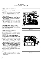
Page 22: ...ch is loaded be cause of any electrical failure manually remove it by taking the following steps 1 Unplug the power cord plug from the power outlet 2 Refer to the disassembly procedure and perform the dis assembly of the major parts before removing the drum assembly 3 Unload the pole base assembly by manually turning the loading motor of the mechanism assembly toward the front In doing so hold the...

Page 23: ... 1 3d 4 In the same way as in the electrical failure instructions in 2 1 3 1 5 remove the top guide 5 Raise the cassette tape cover By keeping it in that posi tion draw out the cassette tape case from the cassette holder and take out the tape 6 By hanging the pinch roller arm assembly spring back on the hook take up the slack of the tape into the cas sette Fig 2 1 3d Fig 2 1 3c Pole base assembly ...

Page 24: ...d Press lever assembly Lid guide Guide arm assembly Reel disk take up side Sub brake assembly take up side Main brake assembly take up side Idler arm assembly Idler lever Main brake assembly supply side Reel disk supply side Rec safety lever Tension brake assembly Adjust pin Tension arm assembly Pole base assembly supply side Full erase head Pole base assembly take up side T1 T26 T25 T24 T23 T22 T...

Page 25: ...y as this will cause damage to the video head 2 To clean the parts of the tape transport system other than the upper drum use a piece of closely woven cloth or a cotton swab soaked with alcohol 3 After cleaning make sure that the cleaned parts are com pletely dry before using the video tape 3 Lubrication With no need for periodical lubrication you have only to lu bricate new parts after replacemen...

Page 26: ...ry encoder B 1 2 2 11 Clutch unit B 1 2 2 12 Change lever assembly B 3 2 2 12 Direct gear B 4 2 2 12 Coupling gear B 5 2 2 12 Clutch gear B 6 2 2 13 Link lever B 1 2 2 14 Cassette gear B 2 2 2 14 Control cam B 2 2 2 14 Worm gear B 1 Lid guide T B 5 2 2 15Control bracket1 B 1 2 2 15Control plate B 6 2 2 16Loading arm gear supply side B 7 2 2 16Loadingarmgear take upside B 8 2 2 16Loading arm gear s...

Page 27: ...ration in response to phases of the rotary encoder internal switch positions the mechanism may not operate properly unless such parts as the rotary encoder control plate loading arm gear control cam cassette gear limit gear relay gear and drive gear are installed in their correct posi tions Especially this model is not provided with any cassette hous ing assembly so that cassette loading and unloa...

Page 28: ...y into the groove See Fig 2 2 3g 4 While swinging the lock lever R of the cassette holder assembly toward the front put the legs A and B into the rail See Fig 2 2 3g 5 Drop the three legs on the left side of the cassette holder assembly into the groove at one time See Fig 2 2 3h 6 Slide the whole cassette holder assembly toward the front to bring it to the eject end position 7 Install the limit ge...

Page 29: ...replacing only the A C head remove the three screws B while controlling the compression spring Fig 2 2 6a Fig 2 2 6c Fig 2 2 4a 2 2 5 Guide arm assembly and press lever assembly 1 How to remove 1 Remove the spring and expand the lug of the lid guide in the arrow indicated direction Then remove the guide arm assembly by pulling it up 2 Remove the press lever assembly by pulling it up See Fig 2 2 5a...

Page 30: ...mbly are correctly in stalled as indicated in Fig 2 2 8b 3 Making sure that the connector for the capstan motor is correctly mounted and securely tighten the three screws A Note When the capstan motor has been replaced with a new one perform recording in the EP or LP mode for at least 2 minutes at normal temperatures immediately be fore starting the FF REW or SEARCH operations Ag ing Spacer Spacer...

Page 31: ...the rotary encoder guide in the arrow indicated direction and remove the change lever assembly 2 Remove the slit washer retaining the direct gear and re move the latter Take care so as not to lose the washer and spring See Fig 2 2 12a 2 2 10 Rotary encoder 1 How to remove 1 Remove the screw A and remove the rotary encoder by pulling it up See Fig 2 2 10a Fig 2 2 10a Rotary encoder Front side Screw...

Page 32: ...t of the rotary encoder guide Mark E Fig 2 2 13c Worm gear Control cam Main deck guide hole Control cam guide hole Cassette gear 2 2 14 Cassette gear control cam and worm gear 1 How to remove 1 Remove the control cam by lifting it 2 Open the two lugs of the cassette gear outward and pull the latter off 3 Remove the belt wound around the worm gear and the loading motor 4 Open the lug of the lid gui...

Page 33: ...embly shaft Section D Section D Section A Hole A 3 Install the control plate so that the section A of the load ing arm gear shaft fits into the hole A of the control plate the section B of the control plate guide into the hole B and the control plate comes under the section C of the rotary encoder guide and the section D of the loading arm gear shaft while press fit the pole base assmebly sup ply ...

Page 34: ...e main deck 3 Remove the lugs B and C of the sub brake assembly take up side from the main deck and remove the sub brake assembly take up side Fig 2 2 19a Spring Sub brake assembly take up side Lug B Lug A Lug C Fig 2 2 20a Lug D Lug C Spring Lug E Lug A Lug B Main brake assembly take up side Reel disk take up side Main brake assembly supply side Notch 2 2 20 Main brake assembly take up side reel ...

Page 35: ...2 Remove the reel disk supply side by loosening in the arrow indicated direction the main brake assembly sup ply side 3 Remove the tension spring on the back of the main deck Then release the lug of the tension arm bearing in the arrow indicated direction and draw out the tension arm assembly See Fig 2 2 21a Fig 2 2 21a Lugs Tension brake assembly Lug of the tension arm bearing Reel disk supply si...

Page 36: ...stall a new washer and upper drum assembly on the drum shaft See Fig 2 2 25a 3 Install the cap to the upper drum assembly 4 Position the collar assembly as indicated in Fig 2 2 25c while controlling its up down movement 5 Secure the collar assembly in position with a hexagonal wrench while pressing its top with the fingers 6 After installation gently turn the upper drum assembly with your hand to ...

Page 37: ...1a 5 Reduce the V PB FM waveform by the tracking opera tion If a drop in level is found on the left side turn the guide roller of the pole base assembly supply side with the roller driver to make the V PB FM waveform linear If a drop in level is on the right side likewise turn the guide roller of the pole base assembly take up side with the roller driver to make it linear See Fig 2 3 1c 6 Make sur...

Page 38: ...scope Measuring point D TP106 PB FM External trigger E TP111 D FF Adjustment part F A C head base Mechanism assembly Specified value G Maximum V PB FM waveform Adjustment tool H A C head positioning tool PTU94010 1 Play back the alignment tape A1 2 Apply the external trigger signal to D FF E to observe the V PB FM waveform at the measuring point D 3 Set the VCR to the manual tracking mode 4 Loosen...

Page 39: ...point D TP106 PB FM External trigger E TP111 D FF Adjustment part F Jig RCU Code 50 Specified value G STOP mode Maximum V PB FM waveform Adjustment tool H Jig RCU PTU94023B 2 3 5 Tension pole position 1 Play back the back tension cassette gauge A 2 Check that the indicated value on the left side gauge is within the specified value G 3 If the indicated value is not within the specified value G perf...

Page 40: ...304 2 320 4 335 IN FF REW OUT PLAY Direct gear Change lever 2 ON HALF REV HALF FF REW OFF Tension arm ON CONTACT OFF Main brake S ON CONTACT OFF Main brake T ON OFF Sub brake S ON OFF Sub brake T ON OFF OFF ON Capstan brake ON OFF Rec safety switch Operation mode ON PLAY ON REV CONTACT OFF C INS Pinch roller SUPPLY CENTER TAKE UP Idler position READY RESET Take up lever ON OFF Guide arm Timer REC ...

Page 41: ...GER OFF Unless otherwise specified all measuring points and adjustment parts are located on the Main board In the Signal column of the adjustment chart Ext S input means the Y C separated video signal and Ext input means the composite video signal input Jig RCU PTU94023B Alignment tape SP stairstep PAL MHPE Alignment tape LP stairstep PAL MHPE L LPF PTU93006 Alignment tape SP stairstep NTSC MHP Al...

Page 42: ...justment tool H Jig RCU PTU94023B 1 Record the signal A2 in the mode B1 and play back the recorded signal 2 Press the channel buttons simultaneously to enter the manual tracking mode This also brings tracking to the center centre 3 Set the VCR to the FWD slow 1 6 mode 4 Transmit the code F from the Jig RCU to adjust so that the noise bar becomes the specified value G on the TV monitor in the slow ...

Page 43: ...5 Release the EVR mode of the VCR by transmitting the code F1 from the Jig RCU again When the EVR mode is released the adjusted data is memorized Fig 3 3 2a EE Y level H rate Specified value G 3 3 2 EE Y level Fig 3 3 3a PB Y level H rate Specified value G 7 Release the EVR mode of the VCR by transmitting the code F1 from the Jig RCU again When the EVR mode is released the adjusted data is memoriz...

Page 44: ...ontroller so that the higher level channel be comes the specified value G of the note B level as shown in Fig 3 3 4b Adjust before recording then con firm it by playing back 10 After adjustment record the signal A3 then playing it back again At this time confirm that there is no invert ing phenomenon or noise appearing on the playback screen 11 Release the EVR mode of the VCR by transmitting the c...

Page 45: ...253 A FM External trigger E TP111 D FF EVR mode F1 Jig RCU Code 57 EVR address F2 A 30 Press remote controller 3 and 0 keys Specified value G1 400 100 mVp p G2 More than 250 mVp p Adjustment tool H Jig RCU PTU94023B Digit key remote controller 1 Apply the external trigger signal to D FF E to observe the Audio PB FM waveform at the measuring point D 2 Record the signal A3 with no audio signal input...

Page 46: ...t F C3025 TIMER CLOCK Specified value G 1024 008 0 001 Hz 976 5549 0 0010 µsec 1 Connect the frequency counter to the measuring point D1 2 Connect the short wire between the short point D2 and Vcc 5V 3 Short the leads of capacitor D3 once in order to reset the microprocessor of the SYSCON 4 Disconnect the short wire between the short point D2 and Vcc then connect it again 5 Adjust the Adjustment p...

Page 47: ... Alignment tape colour bar SP mode normal VHS mode 2 Audio circuits REC 1KHz 8 dBs sine wave signal in SP mode normal VHS mode PB REC then playback it 3 Movie Camera circuits Measured using a correctly illuminated gray scale or colour bar test chatrs in the E E mode 4 Indication on schematic diagram Waveform indications on the schematic diagram are as shown below 5 Waveform indications Waveform nu...

Page 48: ... 6 Signal path Symbols The arrows indicate the signal path as follows Playback signal path Playback and recording signal path Recording signal path including E E signal path Capstan servo path Drum servo path Example R Y Y Playback R Y signal path Recording Y signal path 7 Indication of the parts for adjustments The parts for the adjustments are surrounded with the circle as shown below 8 Indicati...

Page 49: ... D_Y V_IN GND D_C_OUT GND D_C_IN D_Y_OUT GND D_C_OUT D_Y V_IN GND D_C_IN GND D_A_PB R D_A_REC R GND D_A_PB L GND GND D_A_REC L SW5V NC GND GND GND 12V GND GND 5V CH 12V RF5V BT2 GND GND GND SW12V AL12V AUDIO SW5V SW5V 2 48V AL5 8V GND SWD_Y SWD_C GND TERM_D_C GND TERM_D_Y GND TERM_C_OUT GND GND TERM_Y_OUT CHARA_DATA REAR2_V_IN GND REAR1_V_IN GND REAR1_C_IN GND REAR1_Y_IN REAR2_V_IN GND REAR1_V_IN ...

Page 50: ...U 2SD2144S UV 16 10 CP ICP N20 1SS133 1SS270A IN OUT GND REF PQ15RW11 MTZJ12A RD12ES B1 10 50 16 1A3G 11ES2 ERA15 02 2SD2528 QP 2SD1819A RS 2SC4081 RS 2PC4081 R DTC114EUA UN5211 RN1302 PDTC114EU 50 10 50 RD5 1JS B2 MA4051N M 1SS133 1SS270A 2SD2375 QP 2SD1819A RS 2SC4081 RS 2PC4081 R 50 RD5 1JS B2 MA4051N M 1SS133 1SS270A 10 REGULATOR 0 2 D5204 IC5101 C5104 C5206 D5207 D5303 R5306 R5311 C5210 C5211...

Page 51: ...CN2001 R68 R69 Q2062 C2061 T2052 Q2061 R2062 R2061 C2062 C2063 C2064 R2064 R2063 R2020 CN2002 FULL_E_ON L R2065 FMA_OUT R C2228 R2228 R2229 C103 C93 L17 Q41 BS_P CTL MESECAM H D3 C96 R76 R75 R77 L12 L5 R79 R113 B37 0Ø K2253 K2252 C2230 C2229 R2230 R2231 B2101 D6 R81 R82 R84 R85 R409 R88 R80 B26 C94 C2256 B49 B48 B50 C130 180p 8p 6 8k 220 68µ 0 1 0 1 0 1 0 1 0 01 0 1 1 3 3 2 2 1 3 3 10µ 2 2 1 100 0...

Page 52: ...PEN OPEN OPEN OPEN 16 T OPEN DTC144WU OPEN OPEN OPEN 6 3 T OPEN DTC144WU OPEN OPEN OPEN OPEN OPEN OPEN OPEN OPEN OPEN VSS CLK VCC DATA2 N REC L EE L 5PB L SW1 SW2 P CTL H LED5 LED1 LED2 LED3 LED4 FULL_E_ON LED6 BU2090FS S 80727AN DQ X OPEN 2SD1819A QRS 2SC4081 QRS 2PC4081 R VCC GND Vref LMC1 LMC2 LDM1 LDM2 BA6956AN 16 LDM2 LDM1 PTZ NV16 PTZ NV16 SHORT QAX0527 1 4W LNB2301L01VI 1N4148M 1SS133 GP3S1...

Page 53: ... OPEN EU EK MS OPEN X X X US DOM X X OPEN OPEN OPEN X X X 4 7k 4 7k 4 7k 4 7k 4 7k X X X 6 8k X 4 7k 4 7k X X 10k X X X X X X X 0Ω X 1k 1k 1k 1k 16k 8k 8k 1k 1k 1k OPEN OPEN OPEN OPEN OPEN OPEN QAX0444 QAX0444 QAX0444 X X X 10p 10p 10p 12p 12p 12p X X X X X X X X X X X X X X X X X X X X 1 6pin 1 6pin 1 6pin X X X X X X OPEN OPEN OPEN OPEN OPEN OPEN 1k 1k 1k X X X X X X X X X X X 1 18pin 1 18pin 1 ...

Page 54: ...V_IN REAR1_C_IN FRONT_C_IN 2Fsc TO_PS_C CN701 CN702 L713 Q727 R782 R781 Q728 R783 C780 C781 R780 L712 IC709 C782 C783 R784 B730 B729 B728 C805 C806 IC713 C804 C710 B701 B715 B716 R768 B714 I2C_DATA2 I2C_CLK2 P MUTE L OSD_DATA OSD_CLK OSD_CSB IC708 4 7µ 0 01 33k 22k 270 560 560 47 82 6 8k 3 9k 680 0 01 47 1 5k 0Ω 270 470 2 2k 2 2k 470 470 1k 1M 0 01 100p 1M 0 01 0 01 0 01 0 01 100p 0 01 2 2 100p 2 ...

Page 55: ...k 10k 10k 10k 10k 220 220 220 220 10 10k 220 2 2k 10k 2 2k 10k 220 10 220 0Ω VCC VCC BA15218F B A X2 X1 X X0 X3 VDD Y0 Y2 Y Y3 Y1 INH VEE VSS BU4052BCF 16 B A X2 X1 X X0 X3 VDD Y0 Y2 Y Y3 Y1 INH VEE VSS BU4052BCF 16 B A X2 X1 X X0 X3 VDD Y0 Y2 Y Y3 Y1 INH VEE VSS BU4052BCF 16 VCC VCC BA15218F LA7151 16 16 16 16 16 16 OPEN OPEN OPEN 16 16 VCC VCC BA15218F 16 50 16 B A X2 X1 X X0 X3 VDD Y0 Y2 Y Y3 Y...

Page 56: ... DET_OUT M N GND B BACK H P SAVE OUT1_L2 H OUT1_D H RCA_A OUT R RCA_A OUT L GND TO SYSCON AUDIO I O SW5V SW12V M12V AL5V SW12V GND AL12V DET_IN RF5V 48V DET_OUT W AL5 8V SW5V DRUM12V M12 17V GND M DC3 5V 29V AFC_IN DC3 5V P CTL H V_UP H P SAVE L BS_SW5V AL17V AL6V I2C_DATA2 I2C_CLK2 PAUSE TERM_Y_OUT TERM_C_OUT TUNER_VIDEO REAR2_Y_IN TERM_D_Y REAR2_C_IN TERM_D_C F AUDIO L F AUDIO R FRONT_V_IN SWD_Y...

Page 57: ...11087 PB11087 PB11076 PB11076 R6551 R6552 Q6551 D6551 C6551 C6552 9V REG C6553 C6554 C6555 DEMOD REG PASS CON SW12V B6607 DEMOD OUT R6508 R6510 R6509 R6511 C6519 C6520 MUTE Q6501 Q6502 TUNER MONO B6510 R6553 R6554 B6552 B6554 B6563 B6565 B6566 DEMOD SELECTION R6020 R6023 470 470 470 470 R6021 R6024 TU CE R6022 C6022 470 470 SYSTEM SW R6060 R6061 SYMBOL EU EK FRANCE MS JAPAN DVS2 HDS1 US DVS2 VS20 ...

Page 58: ...C1451 D1402 B1409 C1466 C1467 C1469 C1468 Q1406 R1405 Q1404 IC1401 R1454 1 470 10 1 8k 100k 470 6 8µ 0 1 39p 0 01 33k 39k 10µ 330 33p 68p 220 2 2k 2 7k 1µ 1 5k 820 0 1 0 01 100 6 8k 680 330 0 1 0 1 0 1 0 1 6 8µ 68p 0 1 33p 560 0 1 4 7 680 27k 0 1 0 1 0 1 820 1 3 9k 0 1 0 1 0 1 15k 22k 6 8k 10k 0 1 0 1 0 1 0 1 1 8k 2 2k 1 5k 33µ 22p 39p 6p 51 0 1 0 01 33 27k 1K 10K 0 1 0 1 680 1k 1k 470 470 1k 1k 1...

Page 59: ... 7µ 47 0 1 75 0 01 0 01 0 01 0 01 10 0 1 0 1 75 330 330 0 01 100 4 7µ 0 47 100 27p 0 01 0 01 470 560 1k 0 01 47 47 0 01 33p 0Ω 330 10k 15k 330 68 75 75 0Ω 680p 680p 4 7µ 4 7µ 100 100 4 7µ 4 7µ 100 100 0 001 0 001 100 0 1 100 1µ 33p 0 1 0 1 100 100 0 1 10 10 10 100 100 0 1 0 01 100 0 1 100 100 1µ 6 8k 470 2 7k 0Ω 1k 4 7k 3 3k 1 47 75 75 680p 680p 4 7µ 4 7µ 100 100 4 7µ 4 7µ 100 100 0 001 75 1k 4 7µ...

Page 60: ...00 0 01 0 01 0 22 680k 1k 1k 22k 22k 0 0068 0 0068 2 2 2 2 600 47 0 01 10 10 0 01 2 2 600 0 01 3 9k 6 8k 1µ 0 0022 47 270 0 001 150 3 3µ 1k 0 01 10k 5 6k 5 6k MSP34VCDT 16 CH CH CH CH CH 1SS133 1N4148M 50 50 16 16 50 I2C_DATA I2C_CLK TU_A_MUTE DEMOD_ R DEMOD_ L SW5V GND COMP SIF NC 2SC3936 BC AVSUP ANA_IN1 ANA_IN TESTEN XTAL_IN XTAL_OUT TP D_CTR_OUT1 D_CTR_OUT0 ADR_SEL STANDBYQ I2C_CL I2C_DA TP TP...

Page 61: ...0 50 50 25 25 50 N 25 EE L I2C_DATA I2C_CLK Fsc SW5V SW5V GND GND GND GND C_TO_DIGI Y V_TO_DIGI Y_FROM_DIGI C_FROM_DIGI PB_COLOR V PULSE SECAM_PB_COLOR MAIM_ALC_DET Y_TO_SUB P MUTE L WIDE_DET FRONT_Y_IN FRONT_C_IN FRONT_V_IN REAR2_V_IN V_TO_OSD CHARA_DATA Y_TO_AV V_FROM_AV REC_COLOR REAR1_Y_IN REAR1_C_IN REAR2_Y_IN REAR2_C_IN Y_OUT C_OUT V_FROM_OSD BIAS_FOR_C_OUT GND GND GND GND GND GND 50 25 OPEN...

Page 62: ...4 R876 C872 R877 C873 R878 C875 C876 0Ω 4 7k 47 0 01 3 3k 470 180k 0 1 8 2k 2 7k 15k 470p 680 0 022 4 7µ 2 2 10k 0Ω 0 22 1 10k 1 0Ω 22µ 56p 0 47 10µ 330 0 1 0Ω 0Ω 330 1µ 10k 10k 10p 33µ 0Ω 100 100 1 5k 0Ω 33p 33p 22µ 0Ω 100 100 0 22 5 1k 0 1 1 8k 47 5 6k 0 22 220 OPEN OPEN OPEN OPEN OPEN NC NC OPEN OPEN OPEN OPEN OPEN 2Fsc OSD_CS S CLK S DATA_FRSYS I2C_CLK2 I2C_DATA2 SWD_S DATA CHARA_DATA P MUTE L...

Page 63: ... 15k 330 330 330 2 7k 4 7k 6 8k 39k 1 8k 1 2k 10k 2 2k 2 7k 1 8k 15k 1 8k 1 2k 10k 330 330 330 1 2k 15k 39k 2 2k 2 7k 4 7k 6 8k 15k 100 10kΩ 0 01 10 10 680p 680p 75 0Ω 75 0 01 75 DV HDR RECLINK VHS 6 3 28V DC DC RC_IN GND C BU_GND STB S_DATA_FRSYS S_DATA_TOSYS S_CLK AL5V RCU_5V LED1 LED2 LED3 LED4 LED5 LED6 DTC114E 6 3 S11 S16 VDD S15 S14 S13 S12 S5 S6 G5 G4 G3 G2 G1 S1 S2 S3 S4 S7 S8 S9 S10 VDD X...

Page 64: ... D3 3V D2 5V A2 5V DGND D5V D3 3V D5V DGND 100 0 1 100 0 1 100 0 1 0 1 100 10 100 0 1 0 1 100 10 0 1 100 0 1 0 1 100 0 1 0 1 100 AL5V GND AL3 3V AL3 3V GND AL2 5V AL2 5V GND AUDIO OPEN SI 3018LS NQR0339 001 16 16 NQR0339 001 NQR0339 001 6 3 6 3 6 3 OPEN NQR0339 001 NQR0339 001 6 3 6 3 6 3 6 3 NQR0339 001 OPEN OPEN 6 3 OPEN 6 3 NQR0339 001 NQR0339 001 OPEN OPEN OPEN T T T T TO AUDIO AD DA TO VIDEO ...

Page 65: ...46 C8648 C8649 DVIDEO1 DVIDEO2 DVIDEO3 DVIDEO4 DVIDEO5 DVIDEO6 DVIDEO7 CLK27MV VR8602 DGND OUTY3 OUTY2 OUTY1 OUTY0 OUTC3 OUTC2 OUTC1 OUTC0 XRSTVDEC JVSDI JVCS 10 820 390 33k 22k 820 1 8k 1k 0 1 10 750 15p 15µ 33µ 8p 39p 33p 2 2k 470 0 01 0 01 2 2k 22k 27k 4 7k 1k 0 1 1k 750 15p 15µ 33µ 330 8p 39p 33p 330 1 5k 0Ω 0 1 820 33µ 15µ 2 2k 33p 39p 8p 750 15p 1k 0 1 1k 390 820 820 22k 27k 0 01 220 100 0 0...

Page 66: ... DA_SCLK DA_LRCLK DEM0 DEM1 XRSTDEC 4 7 0Ω 1 0 1 0 1 0 1 15k 15k 1 150p 150p 0Ω 0 1 0Ω 1k 1k 0Ω 1k 1k 2 2k 2 2k 10 3k 3k 1k 0Ω 0Ω 1k 10 4 7 47 0 0033 0 0033 47 0 0068 0 0068 10k 10k 220 220 22 4 7 8 2k 8 2k 0 1 0 1 10µ 0 1 0 1 10 22 0Ω 1 1 10µ 0Ω 0Ω 0Ω 0Ω 6 3 50 OPEN OPEN 50 A_IN R A_OUT L A_OUT R AGND AGND AGND AGND A_IN L VA VCML VB AGND VCOM AOUTR AOUTL DEM0 DEM1 CMODE SDTI VD DGND VRDA VRAD AI...

Page 67: ...Vssio Vssio Vssio Vssio Vssio Vssio Vssio Vssio Vssio Vssio Vssio Vssio MA9 MA8 MA7 MA6 MA5 MA4 MA3 MA2 MA1 MA0 MA10 MA11 MA12 MA13 MCLK CKE CS0 CS1 RAS CAS WE DQM1 DQM0 DQM2 DQM3 AD0 AD1 AD2 AD3 AD4 AD5 AD6 AD7 AD8 AD9 AD10 AD11 AD12 AD13 AD14 AD15 AD16 AD17 AD18 AD19 AD20 AD21 AD22 AD23 AD24 AD25 AD26 AD27 AD28 AD29 AD30 AD31 LA0 LA1 LA2 LA3 ALE RD ACK SCLK PWE3 PWE2 PWE1 PWE0 LHLDA LHLD RXD1 SS...

Page 68: ...1 D12 D13 D14 D15 D7 D6 VSS VDDE D5 D4 D3 VDDI D2 D1 D0 VDDE VSS ADRS27 ADRS26 ADRS17 ADRS16 ADRS15 XSPRAS XSPCAS XSPWE VDDI SPSDCLK SPCKE VSS VDDE ADRS5 ADRS6 ADRS7 ADRS8 ADRS9 ADRS10 ADRS11 VDDI VDDE VSS ADRS4 ADRS3 ADRS2 ADRS12 ADRS13 ADRS14 VSS VDDE DVIDEO0 DVIDEO1 DVIDEO2 DVIDEO3 DVIDEO4 DVIDEO5 DVIDEO6 DVIDEO7 VDDI XVALID FIELD XVSYNC XHSYNC VCLK VDDE VSS SDDATA8 SDDATA9 SDDATA10 SDDATA11 SD...

Page 69: ... CS BA A10 A0 A1 A2 A3 VDD VSS DQ15 DQ14 VSSQ DQ13 DQ12 VDDQ DQ11 DQ10 VSSQ DQ9 DQ8 VDDQ N C RFU UDQM CLK CKE N C A9 A8 A7 A6 A5 A4 VSS KM416S1120DT G8 OPEN OPEN SYSRST GND DD7 DD8 DD6 DD9 DD5 DD10 DD4 DD11 DD3 DD12 DD2 DD13 DD1 DD14 DD0 DD15 GND KEY DMARQ GND DIOW GND DIOR GND IORDY CSEL DMACK GND INTRQ RESERVED DA1 PDIAG DA0 DA2 CS0 CS1 DASP GND NSW0100 001X OPEN 47p NQR0339 001X OPEN OPEN OPEN ...

Page 70: ...2 C8 C9 R3 R4 TL13 TL12 TL11 C10 R5 R1 R2 TL1 TL2 TL3 TL4 TL5 TL6 TL7 TL8 TL9 TL10 RA1 RA2 10 0 1 0 1 0 1 0 1 0 1 0 1 0 1 10 10k 10k 0 1 1k 1k 1k 0 0Ω EPM3064ATC44 10 uPD485505G 25 DVIDEO0 DVIDEO1 DVIDEO2 DVIDEO3 DVIDEO4 DVIDEO5 DVIDEO6 DVIDEO7 D3 3V D3 3V D3 3V CLK27M DGND DGND DGND GND GND A5V A5V DVIDEO_0 DVIDEO_2 DVIDEO_1 DVIDEO_3 DVIDEO_4 DVIDEO_5 DVIDEO_6 DVIDEO_7 NQR0339 001X 6 3 NQR0339 00...

Page 71: ...20 PT00 P13 T10 P12 INT2 P11 INT1 XT2 NC XT1 P10 INT0 P63 KR3 P70 KR4 P71 KR5 RESET S0 S1 S2 S3 S4 S5 S6 S7 S8 S9 S10 S11 COM0 COM1 COM2 COM3 VCL0 VCL1 VCL2 P40 P41 P42 P43 VSS P50 P51 P52 P53 BIAS P00 INT4 P01 SCR 1 12 2 3 5 4 6 8 7 9 10 11 13 14 16 15 17 19 18 20 21 22 23 24 25 26 27 28 S0 S1 S2 S3 S4 S5 S6 S7 S8 S9 S10 S11 S12 S13 S14 S15 S16 S17 S18 S19 COM0 COM1 COM2 COM3 P03 SI SB1 P02 SO SB...

Page 72: ...c DIV SYSCON CN3001 4 D PG CN3001 5 D FG VIDEO WF7 TP2253 A PB FM PB 0 6 Vp p 50 mV 5 msec DIV WF5 TP111 D FF REC PB 4 3 Vp p 0 1 V 10 msec DIV WF3 TP106 PB FM PB 0 52 Vp p 20 mV 5 msec DIV AUDIO CN3003 2 CAP_FG WF11 CN512 4 REC PB 1 6 Vp p 50 mV 20 µsec DIV WF7 CN511 25 REC PB 2 2 Vp p 50 mV 20 µsec DIV WF8 CN511 27 REC PB 0 52 Vp p 20 mV 20 µsec DIV WF9 CN511 29 PB 0 5 Vp p 20 mV 20 µsec DIV WF1...

Page 73: ...EC PLAY PIN NO MODE REC PLAY PIN NO MODE REC PLAY PIN NO MODE REC PLAY PIN NO MODE REC PLAY PIN NO VIDEO AD DA 8 10 8 10 8 9 4 8 4 8 10 0 1 0 1 11 4 8 4 8 12 0 0 13 4 5 4 5 14 4 4 4 4 15 4 8 4 8 16 4 8 4 8 17 4 8 4 8 18 4 8 4 8 19 10 8 10 8 20 2 3 2 3 21 1 3 1 3 22 1 4 1 4 23 2 6 2 6 24 2 0 2 0 CN7101 1 1 1 1 1 2 0 0 3 2 0 2 0 4 0 0 5 5 6 5 6 6 0 0 7 1 3 1 3 8 0 0 9 1 1 1 1 10 0 0 11 1 5 1 5 12 0 ...

Page 74: ... 3 31 3 3 3 3 32 3 3 3 3 33 0 0 34 0 0 35 1 7 1 7 36 0 0 37 0 0 38 3 3 3 3 39 3 3 3 3 40 3 3 3 3 41 0 0 42 3 3 3 3 43 3 3 3 3 44 3 3 3 3 45 3 3 3 3 46 3 3 3 3 47 0 0 48 3 3 3 3 49 3 3 3 3 50 0 0 IC8403 1 3 3 3 3 2 3 3 3 3 3 3 3 3 3 4 0 0 5 3 3 3 3 6 3 3 3 3 7 3 3 3 3 8 3 3 3 3 9 3 3 3 3 10 0 0 11 3 3 3 3 12 3 3 3 3 13 3 3 3 3 14 3 3 0 15 0 3 3 16 3 3 3 3 17 3 3 3 3 18 3 3 3 3 19 3 3 3 3 20 3 3 3 3...

Page 75: ...AL5 8V 1 2 HEAD HEAD A C TO A C CTL CN1 VIDEO AUDIO 1 2 6 CTLAMPOUT CTL HEAD CTL HEAD CTL CTL SERIAL MEMORY SW1 SW2 15 4 6 FULL_E_ON L N REC L TO SW REG I2C_CLK2 I2C_DATA2 FLY_REC H CAP_REV L CAP_CTL_V CAP_FG DRUM_CTL_V VIDEO_ENV S DATA_FRSYS S DATA_TOSYS S DATA_FRSYS V_UP H OSD CS I2C_CLK_A V I2C_DATA_A V I2C_DATA_A V I2C_CLK_A V FRONT H D_TU H TU_DATA TU_CLK SP_FG S DATA_TOSYS END_SENSOR START_S...

Page 76: ...SCON FL E Y YING A FF DEMOD R DEMOD L R_IN L_IN FRONT_A R FRONT_A L VIDEO AUDIO SIGNAL PROCESSOR A MUTE H R CH R CH DEC R DEC L LINE OUT R LINE OUT L LOG L LOG R A MUTE H I2C_DATA_A V I2C_CLK_A V A ENV ND L H REC_ST H FULL_E_ON L N REC L MAIN VIDEO AUDIO AUDIO I O CONNECTION 1 A OUT R 2 A IN R 3 A OUT L 4 A GND 6 A IN L AV1 IN OUT TERMINAL 0 6 2 A IN A OUT R R 1 A GND 4 A OUT 3 L A IN 6 L 4 3 2 1 ...

Page 77: ... USED NOT FILTER FILTER 1 5 S SUB 4 BPF BUF com CNR PS REC PB 24 29 31 CIN REC PB COMB 3L PB BPF Q1408 Q1418 Q1420 BUF BUF Q1417 LPF 19 17 BUF Q1406 Y C SEP MIX REC 0 5 COUT Q1402 3D YOUT Y COMB SDATA SCLK 11 12 21 22 20 18 17 23 25 26 27 29 30 16 14 13 12 11 10 9 3 2 1 2 4 6 8 10 12 14 CN512 4 14 15 13 12 11 16 17 18 I2C DATA A V EE L I2C CLK A V Fsc C TO DIGI Y V TO DIGI Y FROM DIGI C FROM DIGI ...

Page 78: ...LPF REC DO SQPB SQPB SQPB EQ ET ET ET LPF Det2 LEVEL 2 1 L SECAM L SECAM C BDL P R CLK 7 112 111 104 101 120 38 SW1 Head SW2 Head HPF TANC ME SECAM DET Comp 40 X tal 42 34 2fsc REC AFC PB APC Killer Color Det ID ACC Det REC APC CR Det VCO OSC PB REC Discri DET ENV 105 106 SP1 108 109 110 8 DET DET CH2 CH1 CH2 CH1 REC YCA L SECAM P R 629 TRAP MUTE SP 2FL DOWN Conv LPF 2M P R 4Phase Gen CTL HPF fH T...

Page 79: ...31 VIO0 VIO7 VIO0 VIO7 126 131 133 134 32 8 AD0 AD31 163 168 172 176 178 180 ADATA 200 74 AOUT0 136 139 141 144 146 148 153 155 157 158 16 IC8206 IC8207 D LATCH D0 D7 IC8204 FLASH ROM Q0 Q7 A4 A19 D0 D15 IC8201 IC8202 IC8203 12 13 15 MA0 MA13 A0 A11 BA0 BA1 14 20 26 29 35 MD0 MD31 DQ0 DQ15 32 2 4 5 7 8 10 11 13 SDRAM 16 18 20 21 25 26 28 29 30 32 33 2 3 5 7 9 43 45 46 48 50 52 54 56 58 61 63 64 22...

Page 80: ...ATTERY 307 BATTERY X2 R6 TYPE 308 QPC02202230P POLY BAG 310 LPT0606 001A INST BOOK EN HDS1EU REF No PART No PART NAME DESCRIPTION REF No PART No PART NAME DESCRIPTION SPEC OF BARCODE 301 FINAL ASSY M2 ADHESIVE TAPE 307 308 306 306A 302 303 302 311 312 316 HDS1EU 317 HDS1EK SPEC OF BARCODE 310 315 314 LPT0606 002A INST BOOK GE HDS1EU LPT0606 003A INST BOOK FR HDS1EU LPT0606 004A INST BOOK DU HDS1EU...

Page 81: ... 564 511 517 526 Y T S 533 533 538 561 539 534 511E 511E 511A DIGITAL BOARD ASSY 50 DIGITAL SUB BOARD ASSY 49 M C REGULATOR BOARD ASSY 02 511B 511B 511D 511C 511C 543 L WR9 SW REG BOARD ASSY 01 526 526 538 T N D X X K F Q O Q V V J H B A S E MAIN BOARD ASSY 03 3D DIGITAL 2M BOARD ASSY 05 S SUB BOARD ASSY 15 ON SCREEN BOARD ASSY 17 WR100 Incl 03 553 553 553 553 WR16 501E 501 WR6 G WR18 567 WR2 C D ...

Page 82: ...0413 SPECIAL SCREW MECHA 532 LP40700 001A SPECIAL SCREW MECHA 533 LP40226 001A PC SUPPORT X2 534 PQ21623 2 5 EARTH PLATE RF 535 QYTDSF3010Z SCREW X2 MECHA 538 QYTDSF3010Z SCREW X2 MAIN 539 QYTDST3006Z SCREW MAIN 542 QYTDST3006Z SCREW X4 DIGITAL 543 QYTDST3006Z SCREW X2 SW REG 548 QAR0121 001 FAN MOTOR 549 QYTDSP4030M SCREW X2 550 QYNNS4000Z NUT X2 551 QYWLS4277A0Z SPRING WASHER X2 553 QYTDSF2608Z ...

Page 83: ...1 112 113 151 116 115 117 118 114 119 66 63 68 67 65 64 70 23 25 24 18 19 20 16 27 71 87 22 99 94 96 100 93 97 95 31 80 81 34 37 35 103 32 102 36 38 108 109 90 92 AA AA 69 110 15 84 86 1B 1A 13 12 107 26 13 21 5 6 4 11 3 10 7 AA 14 Classifi Part No Symbol in cation drawing Grease KYODO SH P AA Oil COSMO HV56 BB NOTE This section indicates that the grease and oil are to be applied on locations mark...

Page 84: ...108 002A TENSION ARM ASSY 73 LP30003 010A TENSION SPRING 74 LP40109 003D TENSION BRAKE ASSY 75 PQ46302 1 3 ADJUST PIN 76 LP30232 002A TENSION ARM BEARING 78 LP40532 009B MAIN BRAKE ASSY SUPPLY 80 LP40111 014C MAIN BRAKE ASSY TAKE UP 81 LP30003 029A TENSION SPRING 82 LP40112 001F SUB BRAKE ASSY TAKE UP 83 LP40357 001B TENSION SPRING 84 LP40461 001A CAPSTAN BRAKE ASSY 85 QAR0132 001 CAPSTAN MOTOR 86...

Page 85: ...310 1SS133 DIODE or 1SS270A DIODE D5311 1SS133 DIODE or 1SS270A DIODE D5312 1SS133 DIODE or 1SS270A DIODE D5313 1SS133 DIODE or 1SS270A DIODE R5101 QRG02GJ 683 OMF RESISTOR 68kØ 2W R5102 QRE141J 100Y RESISTOR 10Ø 1 4W R5103 NRSA02J 332X MG RESISTOR 3 3kØ 1 10W R5104 QRE141J 681Y RESISTOR 680Ø 1 4W R5105 QRT01DJ R47X MF RESISTOR 0 47Ø 1W R5107 QRE141J 684Y RESISTOR 680kØ 1 4W R5108 QRE121J 470Y RES...

Page 86: ... RD5 1JS B2 T2 ZENER DIODE or MA4051N M T2 ZENER DIODE D5328 1SS133 DIODE or 1SS270A DIODE D5329 1SS133 DIODE or 1SS270A DIODE D5331 1SS133 DIODE or 1SS270A DIODE D5333 1SS133 DIODE or 1SS270A DIODE D5334 11ES2 DIODE or ERA15 02 T2 DIODE or 1A3G DIODE D5335 1SS133 DIODE or 1SS270A DIODE D5336 MTZJ12A ZENER DIODE or RD12ES B1 T2 ZENER DIODE R5322 NRSA02J 471X MG RESISTOR 470Ø 1 10W R5323 NRSA02J 47...

Page 87: ... 2SA1576A QR X TRANSISTOR or 2PA1576 R X TRANSISTOR Q7 2SD1819A QRS X TRANSISTOR or 2PC4081 R X TRANSISTOR or 2SC4081 QRS X TRANSISTOR Q8 2SD1819A QRS X TRANSISTOR or 2SC4081 QRS X TRANSISTOR or 2PC4081 R X TRANSISTOR Q9 2SB1218A QR X TRANSISTOR or 2PA1576 R X TRANSISTOR or 2SA1576A QR X TRANSISTOR Q10 2SB1218A QR X TRANSISTOR or 2SA1576A QR X TRANSISTOR or 2PA1576 R X TRANSISTOR Q17 DTC144WU TRAN...

Page 88: ...Q3001 2SD1819A QRS X TRANSISTOR or 2SC4081 QRS X TRANSISTOR or 2PC4081 R X TRANSISTOR Q3002 PTZ NV16 PHOTO TRANSISTOR or PTZ NV16A PHOTO TRANSISTOR Q3003 PTZ NV16 PHOTO TRANSISTOR or PTZ NV16A PHOTO TRANSISTOR Q3004 2SD1819A QRS X TRANSISTOR or 2SC4081 QRS X TRANSISTOR or 2PC4081 R X TRANSISTOR Q3005 2SD1819A QRS X TRANSISTOR or 2PC4081 R X TRANSISTOR or 2SC4081 QRS X TRANSISTOR Q3007 DTC144WU TRA...

Page 89: ...J 102X MG RESISTOR 1kØ 1 10W R725 NRSA02J 105X MG RESISTOR 1MØ 1 10W R726 NCB21HK 103X CAPACITOR 0 01µF 50V R727 NRSA02J 105X MG RESISTOR 1MØ 1 10W R767 NRSA02J 0R0X MG RESISTOR 0Ø 1 10W R768 NRSA02J 0R0X MG RESISTOR 0Ø 1 10W R769 NRSA02J 122X MG RESISTOR 1 2kØ 1 10W R770 NRSA02J 471X MG RESISTOR 470Ø 1 10W R771 NRSA02J 471X MG RESISTOR 470Ø 1 10W R772 NRSA02J 102X MG RESISTOR 1kØ 1 10W R773 NRSA0...

Page 90: ...RSA02J 103X MG RESISTOR 10kØ 1 10W R2687 NRSA02J 221X MG RESISTOR 220Ø 1 10W R2688 NRSA02J 221X MG RESISTOR 220Ø 1 10W R2689 NRSA02J 0R0X MG RESISTOR 0Ø 1 10W R2691 NRSA02J 221X MG RESISTOR 220Ø 1 10W R2692 NRSA02J 121X MG RESISTOR 120Ø 1 10W R3011 NRSA02J 0R0X MG RESISTOR 0Ø 1 10W R3012 NRSA02J 0R0X MG RESISTOR 0Ø 1 10W R3013 NRSA02J 0R0X MG RESISTOR 0Ø 1 10W R3016 NRSA02J 0R0X MG RESISTOR 0Ø 1 1...

Page 91: ...02J 102X MG RESISTOR 1kØ 1 10W R4001 NRSA02J 472X MG RESISTOR 4 7kØ 1 10W R4003 NRSA02J 561X MG RESISTOR 560Ø 1 10W R4004 NRSA02J 561X MG RESISTOR 560Ø 1 10W R4005 NRSA02J 562X MG RESISTOR 5 6kØ 1 10W R4007 NRSA02J 102X MG RESISTOR 1kØ 1 10W R4008 NRSA02J 102X MG RESISTOR 1kØ 1 10W R4009 NRSA02J 102X MG RESISTOR 1kØ 1 10W R4010 NRSA02J 102X MG RESISTOR 1kØ 1 10W R4011 NRSA02J 222X MG RESISTOR 2 2k...

Page 92: ... 22pF 50V C65 QEKJ1HM 105 E CAPACITOR 1µF 50V C69 NCB21EK 104X CAPACITOR 0 1µF 25V C70 NCB21EK 104X CAPACITOR 0 1µF 25V C72 NDC21HJ 470X CAPACITOR 47pF 50V C73 NDC21HJ 120X CAPACITOR 12pF 50V C80 NCB21HK 103X CAPACITOR 0 01µF 50V C84 NRSA02J 682X MG RESISTOR 6 8kØ 1 10W C93 NDC21HJ 220X CAPACITOR 22pF 50V C94 NRSA02J 0R0X MG RESISTOR 0Ø 1 10W C103 NCB21HK 103X CAPACITOR 0 01µF 50V C106 NCB21HK 821...

Page 93: ...4X CAPACITOR 0 1µF 16V C2255 NDC21HJ 181X CAPACITOR 180pF 50V C2601 QEKJ1CM 106 E CAPACITOR 10µF 16V C2602 NDC21HJ 101X CAPACITOR 100pF 50V C2603 NDC21HJ 101X CAPACITOR 100pF 50V C2604 QEKJ1CM 476 E CAPACITOR 47µF 16V C2605 QEKJ1CM 106 E CAPACITOR 10µF 16V C2606 QEKJ1HM 105 E CAPACITOR 1µF 50V C2607 QEKJ1HM 105 E CAPACITOR 1µF 50V C2610 NDC21HJ 101X CAPACITOR 100pF 50V C2611 NDC21HJ 101X CAPACITOR...

Page 94: ...U0150 002 TUNER SD1 LP30644 001A SHIELD CASE PRE OT1 LP40229 002A PLATE TU6001 OT2 PU59915 105 500SPACER0 01 PLATE OT3 PU59915 105 500SPACER0 01 WR3002 WR100 QUQ112 1414CG FFC WIRE S SUB WR3002 QUB351 15A4A4 SIN TWIST WIRE CN1 QGF1028C1 13 FPC CONNECTOR 1 13 U DRUM CN703 QGA2001C1 06 CONNECTOR 1 6 DIGITAL CN2001 QGF1207C1 07 FPC CONNECTOR 1 7 A C HEAD CN2002 QGB2532J1 02 CONNECTOR 1 2 FE HEAD CN26...

Page 95: ...X CAPACITOR 0 01µF 50V C1403 QEKJ0JM 337 E CAPACITOR 330µF 6 3V C1404 NCF21EZ 104X CAPACITOR 0 1µF 25V C1405 NCF21EZ 104X CAPACITOR 0 1µF 25V C1406 NCB21HK 103X CAPACITOR 0 01µF 50V C1407 NDC21HJ 680X CAPACITOR 68pF 50V C1408 NDC21HJ 330X CAPACITOR 33pF 50V C1410 QEKJ1EM 475 E CAPACITOR 4 7µF 25V C1411 NCF21EZ 104X CAPACITOR 0 1µF 25V C1412 NDC21HJ 680X CAPACITOR 68pF 50V C1413 NDC21HJ 330X CAPACI...

Page 96: ...ESISTOR 75Ø 1 10W R7126 NRSA02J 101X MG RESISTOR 100Ø 1 10W R7127 NRVA02D 561X CMF RESISTOR 560Ø 1 10W R7128 NRVA02D 471X CMF RESISTOR 470Ø 1 10W R7129 NRSA02J 102X MG RESISTOR 1kØ 1 10W R7130 NRSA02J 0R0X MG RESISTOR 0Ø 1 10W R7131 NRSA02J 153X MG RESISTOR 15kØ 1 10W R7132 NRSA02J 103X MG RESISTOR 10kØ 1 10W R7133 QRE121J 331Y RESISTOR 330Ø 1 2W R7134 QRE141J 680Y RESISTOR 68Ø 1 4W R7135 NRVA02D ...

Page 97: ...69 NCB21HK 103X CAPACITOR 0 01µF 50V C7170 NCB21HK 102X CAPACITOR 0 001µF 50V L7101 QQL29BJ 4R7Z COIL 4 7µH L7102 QQL29BJ 4R7Z COIL 4 7µH L7103 QQL29BJ 4R7Z COIL 4 7µH L7104 QUY153 050Y IM BUS WIRE L7105 QUY153 050Y IM BUS WIRE L7106 QQL071J 4R7Y COIL 4 7µH L7107 QQL071J 4R7Y COIL 4 7µH L7108 QQL071J 4R7Y COIL 4 7µH L7109 QQL071J 4R7Y COIL 4 7µH L7110 QUY153 050Y IM BUS WIRE L7113 QQL071J 1R0Y COI...

Page 98: ... 225 E CAPACITOR 2 2µF 50V C502 QEKJ1EM 475 E CAPACITOR 4 7µF 25V C503 QEKJ1HM 225 E CAPACITOR 2 2µF 50V C504 NCB21EK 104X CAPACITOR 0 1µF 25V C505 QEKJ1EM 475 E CAPACITOR 4 7µF 25V C506 NCB21EK 104X CAPACITOR 0 1µF 25V C507 QEKJ0JM 227 E CAPACITOR 220µF 6 3V C508 QEPF1HM 474 NP E CAPACITOR 0 47µF 50V C509 QEKJ1CM 106 E CAPACITOR 10µF 16V C510 QEKJ0JM 227 E CAPACITOR 220µF 6 3V C511 NCB21HK 103X C...

Page 99: ... 1 10W B851 NRSA02J 0R0X MG RESISTOR 0Ø 1 10W B853 NRSA02J 0R0X MG RESISTOR 0Ø 1 10W B855 NRSA02J 0R0X MG RESISTOR 0Ø 1 10W B857 QUY153 050Y IM BUS WIRE B860 NRSA02J 0R0X MG RESISTOR 0Ø 1 10W B863 NRSA02J 0R0X MG RESISTOR 0Ø 1 10W C851 QEKJ0JM 337 E CAPACITOR 330µF 6 3V C852 NCB21EK 224X CAPACITOR 0 22µF 25V C853 NCB21CK 105X CAPACITOR 1µF 16V C856 NCB21CK 105X CAPACITOR 1µF 16V C857 NDC21HJ 560X ...

Page 100: ...R 10kØ 1 4W C7001 QCFB1HZ 104 CAPACITOR 0 1µF 50V C7002 QETN1HM 106 E CAPACITOR 10µF 50V C7007 QEKC0JM 476 E CAPACITOR 47µF 6 3V C7009 QCSB1HJ 150 CAPACITOR 15pF 50V C7010 QCFB1HZ 104 CAPACITOR 0 1µF 50V C7011 QEKC1AM 227 E CAPACITOR 220µF 10V C7019 QDVB1EZ 223Y CAPACITOR 0 022µF 25V L7001 QUY153 050Y IM BUS WIRE S7001 QSW0456 002Z TACT SWITCH POWER S7002 QSW0456 002Z TACT SWITCH CH S7003 QSW0456 ...

Page 101: ...Y57V161610DTC8 IC IC8003 MN1382 K X IC IC8201 NDV8501VWB IC DIGITAL or NDV8501 2VWA IC DIGITAL IC8202 K4S641632D TC1H IC or HY57641620HGLTH IC or HY57641620HGLTP IC IC8203 K4S641632D TC1H IC or HY57641620HGLTH IC or HY57641620HGLTP IC IC8204 39VF800A7CEK04A IC MICRO C ROM IC8206 SN74LV573APW IC IC8207 SN74LV573APW IC IC8210 TC7WU04FU IC DIGITAL IC8401 MB86390 IC DIGITAL IC8402 KM416S1120DT G8 IC o...

Page 102: ...W R8243 NRSA63J 0R0X MG RESISTOR 0Ø 1 16W R8244 NRSA63J 103X MG RESISTOR 10kØ 1 16W R8245 NRSA63J 103X MG RESISTOR 10kØ 1 16W R8246 NRSA63J 112X MG RESISTOR 1 1kØ 1 16W R8247 NRSA63J 0R0X MG RESISTOR 0Ø 1 16W R8401 NRSA63J 512X MG RESISTOR 5 1kØ 1 16W R8402 NRSA63J 512X MG RESISTOR 5 1kØ 1 16W R8403 NRSA63J 201X MG RESISTOR 200Ø 1 16W R8406 NRSA63J 201X MG RESISTOR 200Ø 1 16W R8407 NRSA63J 332X MG...

Page 103: ...41J 0R0Y RESISTOR 0Ø 1 4W C8001 NCB31CK 104X CAPACITOR 0 1µF 16V C8002 NCB31CK 104X CAPACITOR 0 1µF 16V C8003 NCB31CK 104X CAPACITOR 0 1µF 16V C8004 NCB31CK 104X CAPACITOR 0 1µF 16V C8005 NEA70JM 107X E CAPACITOR 100µF 6 3V C8006 NCB31CK 104X CAPACITOR 0 1µF 16V C8007 NCB31CK 104X CAPACITOR 0 1µF 16V C8008 NCB31CK 104X CAPACITOR 0 1µF 16V C8009 NCB31CK 104X CAPACITOR 0 1µF 16V C8010 NCB31CK 104X C...

Page 104: ...31CK 104X CAPACITOR 0 1µF 16V C8423 NCB31CK 104X CAPACITOR 0 1µF 16V C8424 NCB31CK 104X CAPACITOR 0 1µF 16V C8425 NCB31CK 104X CAPACITOR 0 1µF 16V C8426 NCB31CK 104X CAPACITOR 0 1µF 16V C8427 NCB31CK 104X CAPACITOR 0 1µF 16V C8428 NCB31CK 104X CAPACITOR 0 1µF 16V C8429 NCB31CK 104X CAPACITOR 0 1µF 16V C8430 NCB31CK 104X CAPACITOR 0 1µF 16V C8431 NCB31CK 104X CAPACITOR 0 1µF 16V C8432 NCB31CK 104X ...

Page 105: ...EA71CM 476X E CAPACITOR 47µF 16V C8836 NCB31CK 104X CAPACITOR 0 1µF 16V C8837 NEA71CM 476X E CAPACITOR 47µF 16V C8901 NEA71CM 107X E CAPACITOR 100µF 16V C8902 NCB31CK 104X CAPACITOR 0 1µF 16V C8903 NEA71CM 107X E CAPACITOR 100µF 16V C8904 NCB31CK 104X CAPACITOR 0 1µF 16V C8905 NEA70JM 107X E CAPACITOR 100µF 6 3V C8906 NCB31CK 104X CAPACITOR 0 1µF 16V C8907 NEA70JM 107X E CAPACITOR 100µF 6 3V C8908...

Page 106: ...1016F4 08W FFC FPC CONNECTOR 1 8 MAIN CN8901 QGA2001F2 09V CONNECTOR 1 9 REG LOADING MOTOR BOARD ASSEMBLY 55 PW2 LPA10010 01A2 LOADING MOTOR BOARD ASSY CN1 QGB2533K1 02 CONNECTOR LED BOARD ASSEMBLY 90 PW4 LPA10126 04A4 LED BOARD ASSY D7017 SELU5E20C LE DIODE D7019 QRE141J 103Y RESISTOR 10kØ 1 4W R7056 QRE141J 101Y RESISTOR 100Ø 1 4W C7022 QDYB1CM 103Y CAPACITOR 0 01µF 16V FW7001 QUM022 07A4A4 PARA...

Reviews: