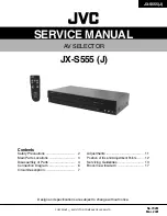
background image

SERVICE MANUAL

AV SELECTOR

No.70251

Mar. 2001

COPYRIGHT      2001 VICTOR COMPANY OF JAPAN, LTD.

Printed in Japan
0103(S)

VICTOR COMPANY OF JAPAN, LIMITED

COMMUNICATION NETWORK BUSINESS UNIT, 1644, SHIMOTSURUMA, YAMATO-SHI, KANAGAWA-KEN, 242-8514, JAPAN
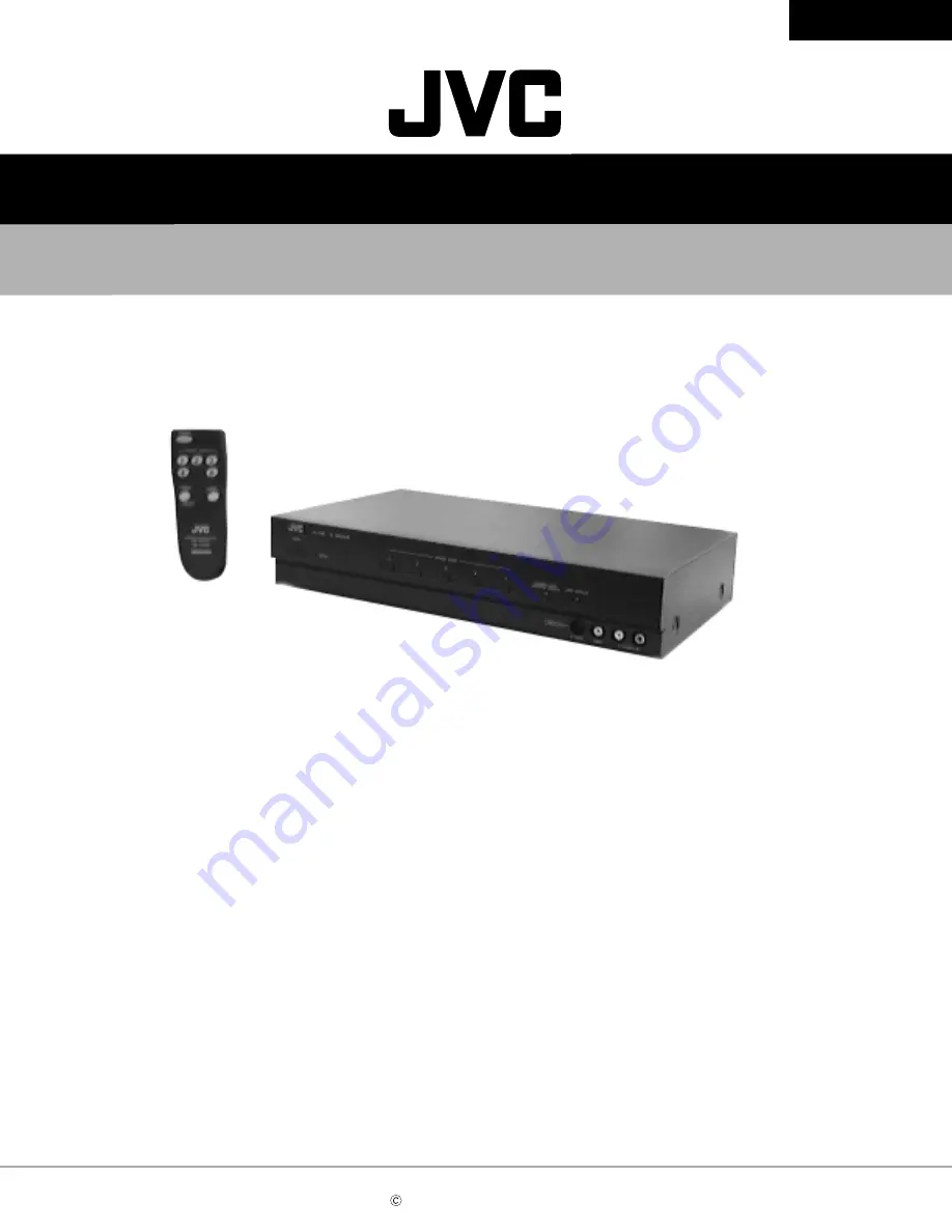
JX-S555 (J)

 No.70251

JX-S555(J)

JX-S555(J)

JX-S555(J)

No.

 70251

Contents

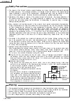
Safety Precautions ...............................

2

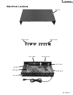
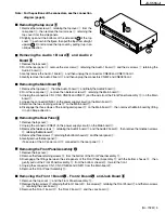
Main Parts Locations ............................ 3
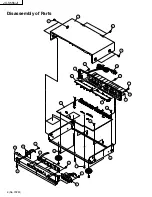
Disassembly of Parts ............................ 4
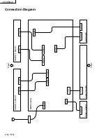
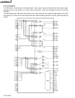
Connection Diagram .............................  6
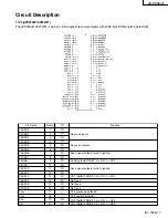
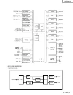
Circuit Description ................................  7

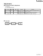
Adjustments ......................................... 11
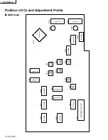
Position of ICs and Adjustment Points ....... 12
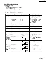
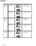
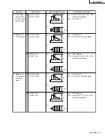
Servicing Guidelines ............................  13
Block View Inside IC .............................  17

Design and specifications are subject to change without notice.

Summary of Contents for JX-S555

Page 1: ...J JX S555 J Contents Safety Precautions 2 Main Parts Locations 3 Disassembly of Parts 4 Connection Diagram 6 Circuit Description 7 Adjustments 11 Position of ICs and Adjustment Points 12 Servicing Guidelines 13 Block View Inside IC 17 Design and specifications are subject to change without notice ...

Page 2: ...hould be confirmed that they have been returned to normal after re assembling 5 Leakage currnet check Electrical shock hazard testing After re assembling the product always perform an isolation check on the exposed metal parts of the product antenna terminals knobs metal cabinet screw heads headphone jack control shafts etc to be sure the product is safe to operate without danger of electrical sho...

Page 3: ... No 70251 3 JX S555 J Main Parts Locations AUDIO 2 board AUDIO 1 board Front 1 board Bottom chassis Front panel ass y Front 2 board Rear panel MAIN board Jack board Top cover ...

Page 4: ...JX S555 J 4 No 70251 Disassembly of Parts 2 17 6 11 18 17 17 5 14 14 16 22 9 8 15 21 22 20 13 19 12 7 4 3 4 1 15 ...

Page 5: ...e Main board B 5 Remove the two clamping screws E on the Main board B 6 Disengage the three claws of the locking card spacer F on the Main board B then remove the Main board by lifting it in an oblique direction Removing the Rear Panel 2 2 2 2 2 1 Removethetopcover1 2 Unplug the connector CN901 in the power supply circuit on the Main board B 3 Remove the twelve screws 7retaining the Audio 1 board ...

Page 6: ...No 70251 Connection Diagram CN702 CN703 CN101 CN701 CN3 CN804 CN806 CN805 CN807 CN808 CN810 CN809 CN813 CN812 CN811 CN901 CN1 AUDIO 2 board Rear AUDIO 1 board MAIN board Front 1 board Front 2 board Jack board Front ...

Page 7: ...3 P56 A14 P57 A15 Vss0 VDD0 P30 P31 Pin No 1 2 3 4 5 6 7 8 9 10 11 12 13 14 15 16 17 18 19 20 Function Key scan inputs Key scan outputs Scan signal outputs for LED lighting Dubbing lock ON OFF H ON L OFF Scan signal outputs for LED lighting CH1 INHIBIT ON OFF H ON L OFF Not used Not used Not used Port grounding potential Port positive potential CH2 INHIBIT ON OFF H ON L OFF CH3 INHIBIT ON OFF H ON...

Page 8: ... used Not used Not used Not used Not used CH5 S1 S2 signal input Not used A D converter reference voltage input Analog power supply for A D converter System reset input Sub system clock oscillation Internally connected To be connected to VSS0 or VSS1 X tal oscillator connection terminals for Main system clock oscillation Grounding potential except for the port CH3 D4 plug insertion detection CH4 D...

Page 9: ... No 70251 9 JX S555 J 2 M101 M102 J46729 002 Comb filter module Buffer VIDEO IN Matrix BPF 1H GDL Buffer Buffer Y OUT C OUT Delay Line ...

Page 10: ...ring the I2 C bus compatibility for TV Among the 5 video inputs 4 inputs are compatible with the S2 and S Video standards The outputs each audio output uses a pair of lines for the L and R channels can be selected independently by the control through the I2 C bus However the second video and audio outputs are always based on the same video and audio input system ...

Page 11: ... Oscillo scope 1 2 Test Point Adjustment Point 2CH C output MONITOR OUT C output Condition Condition Name C output level C output level VR101 VR102 Apply color bar signal to 1CH video input V Apply color bar signal to 1CH video input V Adjust VR101 so that the C output level at 2CH is 0 642 0 02 Vp p Adjust VR102 so that the C output level at MONITOR OUT is 0 642 0 02 Vp p ...

Page 12: ...07 74HC4066AP IC106 74HC4052AP IC402 74HC4052AP IC401 74HC4052AP IC808 74HC4052AP IC809 74HC126AP IC403 NJM 4580D IC801 NJM 4580D IC807 NJM 4580D IC805 NJM 4580D IC804 NJM 4580D IC803 74HC4066AP IC102 74HC4066AP IC104 74HC4066AP IC103 J46729 002 M102 J46729 002 M101 IC101 VR102 VR101 CXA2079Q Position of ICs and Adjustment Points ...

Page 13: ...Q706 or wire is defective 3 Switch operation failure CN3 Pins 8 to 14 0 or 5 V DC NO YES IC2 defective CN701 tack switch or wire defective 5 4 S V switching failure IC101 Pins 7 14 21 and 28 0 V when S Video plug is inserted 5 V when S Video plug is not inserted NO YES PJ107 to PJ110 defective Check IC101 and the surroundings 6 5 Remote control malfunction IC2 Pin 55 5 V DC at remote control code ...

Page 14: ... C Q111 Emitter NO YES Check IC101 and surroundings Check IC102 IC104 and their surroundings F 10 The S Video input at CH5 is not displayed Y Q104 Emitter C Q102 Emitter NO YES Check Q101 to Q104 Q119 Q120 and their surroundings Go to check C G 2 0 Vp p 1 28 Vp p Y C 2 0 Vp p 1 28 Vp p Y C 2 0 Vp p 1 28 Vp p 9 The S Video inputs at CH1 to CH4 are not output at the Monitor output Y Q137 Emitter C Q...

Page 15: ...res 12 Malfunction in Y C separation 2 0 Vp p 1 28 Vp p 2 0 Vp p 1 28 Vp p Y C Y M101 Pin 5 C M101 Pin 3 J NO YES M101 defective Check Q112 to Q114 Q173 Q174 and their surroundings 1 0 Vp p 0 64 Vp p Y C Y Q118 Emitter C Q117 Emitter K NO YES Go to check L Check IC101 and surroundings 13 Malfunction in Y C separation for monitor output 2 0 Vp p 1 28 Vp p Y C Y M102 Pin 5 C M102 Pin 3 L NO YES M101...

Page 16: ...0 32 Vrms Q L IC801 to IC805 Pins 7 R IC801 to IC805 Pins 1 NO YES Check IC801 to IC805 and their surroundings Check IC101 and surroundings 10 dBV 0 32 Vrms 18 Audio signals are not output at the Monitor R L IC807 pins 6 7 R IC807 pins 1 2 NO YES Check IC807 and surroundings Check CN806 and wire 14 Malfunction in Y C mixing of CH1 to CH4 inputs Q107 Emitter Monitor output Q115 emitter NO YES Check...

Page 17: ...P HITACHI 1D 1Q 1Q G1 2 2Q 2Q 2D GND 1 2 3 4 5 6 7 8 16 15 14 13 12 11 10 9 1D C1 3 2 5 6 11 10 13 14 1 4 7 9 12 15 1D G1 2 2D 3D G3 4 4D 1Q 1Q 2Q 2Q 3Q 3Q 4Q 4Q VCC 4D 4Q 4Q G3 4 3Q 3Q 3D TOP VIEW INPUTS TRUE TABLE X Don t care D L H X G H H L OUTPUTS Q L H Qn Q H H Qn LATCH FUNCTION C2 2D 3D C3 C4 4D ...

Page 18: ...JX S555 J 18 No 70251 IC101 CXA2079Q IC102 108 TC74HC4066AP TOSHIBA IC801 807 NJM4580D JRC ...

Page 19: ...BISHI 8 7 6 5 4 3 2 1 M5230L OUTPUT CONTROL INPUT OUTPUT VOLTAGE ADJUSTMENT INPUT OUTPUT BALANCE ADJUSTMENT GND START CIRCUIT OVERHEAT PROTECTOR OUTPUT CONTROL 8 7 REFERENCE VOLTAGE GENERATOR ERROR AMPLIFIER INPUT 6 OUTPUT OVER CURRENT PROTECTOR 5 VOLTAGE ADJUSTMENT 1 GND 2 BALANCE ADJUSTMENT 3 OUTPUT 4 INPUT ERROR AMPLIFIER OVER CURRENT PROTECTOR ...

Page 20: ...4A 8 4Y TOP VIEW A Y IC3 TC74HC04AP TOSHIBA 1G 1 1A 2 1Y 3 2G 4 2A 5 2Y 6 GND 7 14 Vcc 13 4G 12 4A 11 4Y 10 3G 9 3A 8 3Y TOP VIEW INPUTS OUTPUTS G A Y L X Z H L L H H H X Don t Care Z High Impedance R13 Q10 R14 R15 D1 Q9 R17 R16 R1 Q1 R2 R4 R5 Q4 Q3 Q2 R3 Q8 R8 R7 R6 R10 R12 R9 C1 Q13 Q14 Q12 Q5 Q6 R11 Q7 Q11 1 INPUT 2 OUTPUT 3 COMMON INPUT 3 1 2 OUTPUT COMMON TA78L005AP 5V TA78L012AP 12V Schemati...

Page 21: ...Printed in Japan 0103 S VICTOR COMPANY OF JAPAN LIMITED COMMUNICATION NETWORK BUSINESS UNIT 1644 SHIMOTSURUMA YAMATO SHI KANAGAWA KEN 242 8514 JAPAN No 70251 JX S555 J ...

Page 22: ...ode HITACHI D121 1SS120 Diode HITACHI D122 1SS120 Diode HITACHI D123 1SS120 Diode HITACHI D129 1SS120 Diode HITACHI D130 1SS120 Diode HITACHI D131 1SS120 Diode HITACHI D132 1SS120 Diode HITACHI D133 1SS120 Diode HITACHI D134 1SS120 Diode HITACHI D135 1SS120 Diode HITACHI D136 1SS120 Diode HITACHI D141 1SS120 Diode HITACHI D142 1SS120 Diode HITACHI D143 1SS120 Diode HITACHI D144 1SS120 Diode HITACH...

Page 23: ...BISHI Q176 2SA1235 Transistor MITSUBISHI Q401 2SC3052 Transistor MITSUBISHI Q402 2SC3052 Transistor MITSUBISHI Q403 2SC3052 Transistor MITSUBISHI Q404 2SC4432 Transistor SANYO Q405 2SC4432 Transistor SANYO Q406 2SC4432 Transistor SANYO Q407 2SC3052 Transistor MITSUBISHI Q408 2SC3052 Transistor MITSUBISHI Q409 2SC3052 Transistor MITSUBISHI Q410 2SC3052 Transistor MITSUBISHI Q411 2SC3052 Transistor ...

Page 24: ...tor 1 5kΩ 1 10W R162 NRSA02J 152NY M G Resistor 1 5kΩ 1 10W R163 NRSA02J 152NY M G Resistor 1 5kΩ 1 10W R164 NRSA02J 152NY M G Resistor 1 5kΩ 1 10W R165 NRSA02J 102NY M G Resistor 1kΩ 1 10W R166 NRSA02J 681NY M G Resistor 680Ω 1 10W R167 NRSA02J 152NY M G Resistor 1 5kΩ 1 10W R168 NRSA02J 102NY M G Resistor 1kΩ 1 10W R169 NRSA02J 681NY M G Resistor 680Ω 1 10W R170 NRSA02J 123NY M G Resistor 12kΩ 1...

Page 25: ...36 NRSA02J 560NY M G Resistor 56Ω 1 10W R337 NRSA02J 560NY M G Resistor 56Ω 1 10W R338 NRSA02J 560NY M G Resistor 56Ω 1 10W R401 NRSA02J 750NY M G Resistor 75Ω 1 10W R402 NRSA02J 750NY M G Resistor 75Ω 1 10W R406 NRSA02J 224NY M G Resistor 220kΩ 1 10W R407 NRSA02J 224NY M G Resistor 220kΩ 1 10W R408 NRSA02J 103NY M G Resistor 10kΩ 1 10W R409 NRSA02J 103NY M G Resistor 10kΩ 1 10W R410 NRSA02J 222NY...

Page 26: ...579 100 FuseResistor 10Ω VR101 JVPC602 331 Trim Resistor φ6 330Ω VR102 JVPC602 331 Trim Resistor φ6 330Ω C1 J46973 104 Cer Capacitor 0 1uF 25V C4 QER51CM 106G E Capacitor 10uF 16V C5 QER51CM 106G E Capacitor 10uF 16V C6 QETB1AM 107 E Capacitor 100uF 10V C7 NCB31HK 103AY Cer Capacitor 0 01uF 50V C8 NCB31HK 103AY Cer Capacitor 0 01uF 50V C9 NCB31HK 103AY Cer Capacitor 0 01uF 50V C10 NCB31HK 103AY Ce...

Page 27: ... 476 E Capacitor 47uF 16V C402 QER51CM 476 E Capacitor 47uF 16V C403 QER51CM 476 E Capacitor 47uF 16V C404 QER51CM 476 E Capacitor 47uF 16V C405 QER51CM 476 E Capacitor 47uF 16V C406 QER51CM 476 E Capacitor 47uF 16V C407 QETB1AM 107 E Capacitor 100uF 10V C408 QETB1AM 107 E Capacitor 100uF 10V C409 QETB1AM 107 E Capacitor 100uF 10V C410 J46974 105 Cer Capacitor 1uF C411 J46974 105 Cer Capacitor 1uF...

Page 28: ...0 100K Inductor 10uH M101 J46729 002 Y CModule TDK M102 J46729 002 Y CModule TDK A PC901 J46587 001 PhotoCoupler NEC A VD901 J46586 001 Barister A F901 J46830 001 Fuse 1A 125V A for F901 J46595 001 FuseClip A T901 J46831 001 SwitchingTrans X1 JXC0004 000KH X TAL TDK PJ101 J46916 001 PinJack 1PYELLOW PJ102 J46916 001 PinJack 1PYELLOW PJ103 J46916 001 PinJack 1PYELLOW PJ104 J46916 001 PinJack 1PYELL...

Page 29: ... 561NY M G Resistor 560W 1 10W R837 NRSA02J 561NY M G Resistor 560W 1 10W R838 NRSA02J 561NY M G Resistor 560W 1 10W R839 NRSA02J 561NY M G Resistor 560W 1 10W R840 NRSA02J 561NY M G Resistor 560W 1 10W Sub Board Assembly The partwill not be supplied as an assembly R841 NRSA02J 561NY M G Resistor 560W 1 10W R842 NRSA02J 561NY M G Resistor 560W 1 10W R843 NRSA02J 561NY M G Resistor 560W 1 10W R844 ...

Page 30: ...J 473NY M G Resistor 47kW 1 10W C105 QER51CM 476 E Capacitor 47uF 16V C120 NCB31HK 103AY Cer Capacitor 0 01uF 50V C135 QER51CM 476 E Capacitor 47uF 16V PJ701 JMN0YP0 1024G Pin Jack 1PYELLOW PJ702 JMD04P0 1020G Mini Connector 1P PJ703 JMN0YP0 1042G Pin Jack 1P RED PJ704 JMN0YP0 1039G Pin Jack 1P WHITE JWS0106 0221 Conn Wire Assy For CN101 JWS0104 0415 Conn Wire Assy For CN703 Jack Board Assembly Th...

Page 31: ...JX S555 J 10 No 70251 Exploded Views 3 11 8 7 7 11 14 4 10 11 11 10 6 9 9 10 1 11 12 11 12 2 6 Front 1 board Front 2 board MAIN board AC cord AUDIO 2 board AUDIO 1 board Jack board 11 ...

Page 32: ...r 2 KGPS 8RF Main board A 8 J46742 001 Cord Stopper 1 KF 41 9 E74185 002 Foot 4 10 QYSPSF3008Z Tapping Screw 9 Front 1 board Front 2 board and Jack board 11 SPSG3008MY Tapping Screw 45 Rear panel bottom chassis 12 SXST4008M Tapping Screw 4 Top cover 13 QYSPSPL3008Z Screw 3 Heart sink of power unit A 14 J46960 001 Shield Sheet 1 Reverse side of main board ItemNo Parts No Parts Name Q ty Remarks M 1...

Page 33: ...JX S555 J 12 No 70251 Packing Taping Front marking Main unit 3 5 14 11 10 9 8 12 6 4 3 7 2 1 7 ...

Page 34: ...rts No Parts Name Q ty Remarks M 2 M M A Accessories List A 8 J5500 105A Instructions 1 English French and Spanish 9 BT 51005 4 Warranty Card 1 10 BT 51006 1 Registration Card 1 11 PU33941 3 3 JVC Safety Guide 1 12 RM AJ555 Remote Control Unit 1 Enveloped with battery cover 13 J33017 002 Battery Cover 1 For RM AJ555 14 Battery 2 R6 AA ItemNo Parts No Parts Name Q ty Remarks M 3 M M A Parts marked ...

Page 35: ...JX S555 J 14 No 70251 MEMO ...

Page 36: ...TOR S VIDEO MONITOR VIDEO AUDIO 6dB Y C MIXER 6dB S V S V 6dB Y C MIXER 6dB S V S V AUDIO MONITOR Y C SEPARATOR Y C SEPARATOR 1 4 5 1 4 5 1 4 5 1 4 5 LOOP PROTECT 6dB Y C MIXER VIDEO S VIDEO AUDIO AUDIO S VIDEO VIDEO VIDEO S VIDEO AUDIO SOURCE SELECT SOURCE SELECT AUDIO MONITOR OUTPUT2 MONITOR OUTPUT1 OUTPUT1 OUTPUT2 1 4 VIDEO 1 4 S VIDEO AUDIO 1 4 VIDEO MONITOR 1 4 S VIDEO MONITOR AUDIO MONITOR 5...

Page 37: ... 1 7V 5 7V 1 1V 1 7V 5 7V 1 1V 1 7V 5 7V 1 1V 1 6V 1 6V 1 6V 5 7V 6 0V 6 0V 6 0V 5 9V 5 9V 5 9V 1 6V 1 6V 5 7V 1 6V 1 6V 1 6V 5 7V 6 0V 6 0V 6 0V 5 9V 5 9V 5 9V 1 6V 1 6V 1 6V 5 7V 1 6V 1 6V 5 7V 6 0V 6 0V 6 0V 5 9V 5 9V 5 9V 1 6V 1 6V 5 7V 1 7V 0V 4 0V 0V 4 2V 9 0V 3 6V 4 5V 3 2V 4 5V 4 3V 0V 0V 3 5V 3 5V 4 5V 4 0V 4 5V 4 5V 4 0V 4 5V 4 3V 0V 3 2V 3 7V 4 5V 3 6V 4 5V C223 4700u 10v M102 J46729 00...

Page 38: ...5 9V 0V 3 7V 0V 5 9V 0V 0V 6 0V 5 9V 0V 0V 5 9V 0V 0V 5 9V 5 9V 0 9V 0 9V 0 8V 5 2V 6 0V 6 0V 6 0V 5 9V 3 7V 0 9V 0 9V 0 9V 5 2V 6 0V 6 0V 6 0V 5 9V 5 9V 1 0V 1 0V 0 9V 5 2V 6 0V 6 0V 6 0V FROM VIDEO 1 BLOCK FROM CPU BLOCK Notes on this schematic diagram 1 Values are voltages measured with a circuit tester internal resistance 20 k V at respective points of the circuits with the power switch turned...

Page 39: ...V 2 1V 0 9V 5 4V 1 5V 5 5V 6 0V 3 0V 0 7V 0V 5 9V 5 2V 1 4V 5 9V 5 9V 5 9V 2 3V 2 1V 0 9V 5 4V 5 5V 6 0V 3 0V 0 7V FROM CPU BLK Notes on this schematic diagram 1 Values are voltages measured with a circuit tester internal resistance 20 k V at respective points of the circuits with the power switch turned on 2 The circuit diagram printed in this service manual is just a standard The circuitry and c...

Page 40: ... 0V 4 5V 1 8V 0V 4 5V 1 8V A A A FROM AUDIO 1 BLOCK FROM JACK P W B FROM CPU BLK TO AUDIO 2 BLOCK Notes on this schematic diagram 1 Values are voltages measured with a circuit tester internal resistance 20 k V at respective points of the circuits with the power switch turned on 2 The circuit diagram printed in this service manual is just a standard The circuitry and circuit constants are subject t...

Page 41: ... 0V 5 2V 5 3V 5 3V 6 0V 5 3V 5 3V 6 0V 5 9V 5 3V 6 0V A IC2 UPD780021ACWW01 TO FRONT 1 BLOCK TO FRONT 2 BLOCK C5 10u 16V C4 10u 16V TO COMPONENT BLK TO VIDEO 1 BLK Notes on this schematic diagram 1 Values are voltages measured with a circuit tester internal resistance 20 k V at respective points of the circuits with the power switch turned on 2 The circuit diagram printed in this service manual is...

Page 42: ...s marked with A in the shaded area are important as safety parts When replacing them make sure to use the specified parts to ensure safety Notes on this schematic diagram 1 Values are voltages measured with a circuit tester internal resistance 20 k V at respective points of the circuits with the power switch turned on 2 The circuit diagram printed in this service manual is just a standard The circ...

Page 43: ...4 5V 0V 5 1V 4 5V 0V 5 1V 0V 5 1V 1 8V C422 10u 16V 5 3V 1 7V 1 7V 5 3V 1 7V 1 7V 5 3V 1 7V 0V 1 1V 1 7V 0V 2 1V 1 7V 0V 1 4V 1 7V 0V 5 2V 5 3V 0V 5 9V 5 9V 0V FRONT 1 BLOCK FRONT 2 BLOCK AUDIO 1 BLOCK JACK P W B AUDIO 2 BLOCK ...

Page 44: ... No 70251SCH 9 JX S555 J Circuit Boards MAIN BOARD J22026 001 ...

Page 45: ...C130 H2 C131 H2 C132 H2 C133 H2 C134 H2 C136 I2 C137 I3 C138 I3 C14 D5 C140 G2 C141 G2 C142 G1 C143 F1 C145 I5 C146 H3 C147 I4 C148 H5 C149 H4 C15 D5 C150 I2 C151 H3 C152 I4 C153 F1 C154 G2 C155 I4 C156 I5 C157 C2 C159 G4 C16 D5 C160 I3 C161 H3 C162 G1 C163 D2 C164 I5 C165 I4 C167 I4 C168 I5 C169 G5 C17 D5 C170 G5 C171 F5 C172 F5 C175 I3 C176 I4 C18 D5 C183 C3 C184 C2 C187 E1 C189 D1 C19 D5 C193 C...

Page 46: ...801 B3 C802 C3 C803 C3 C804 D3 C805 D3 C806 D3 C807 E3 C808 F3 C826 B2 C827 C2 C828 C2 C829 C2 C830 D2 C831 D2 C832 D2 C833 E2 C834 F2 C835 F2 Others CN701 A1 CN702 A2 CN807 C2 CN808 C2 CN809 D3 CN810 E3 J1001 A1 J1002 A1 J1003 A1 J1004 A1 J1005 A1 J1006 A1 J1007 B1 J1008 B1 J1009 B1 J1010 C1 J1011 C1 J1012 C1 J1013 C1 J1014 D1 J1015 D1 J1016 D1 J1017 E1 J1018 A2 J1019 E2 J1020 E2 J1021 E3 J1022 E...

Reviews: