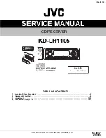
SERVICE MANUAL
COPYRIGHT © 2003 VICTOR COMPANY OF JAPAN, LTD.
No.49827
2003/04
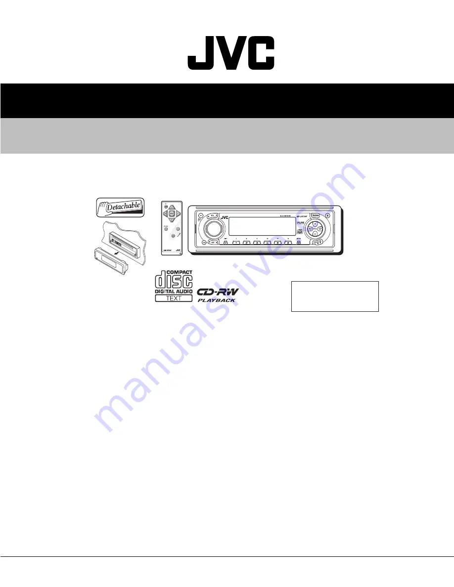
KD-LH1105
CD RECEIVER
49827
2003
04
KD-LH1105
TABLE OF CONTENTS
1
Important Safety Precautions . . . . . . . . . . . . . . . . . . . . . . . . . . . . . . . . . . . . . . . . . . . . . . . . . . . . . . . . . . . 1-2
2
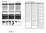
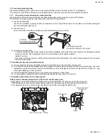
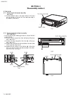
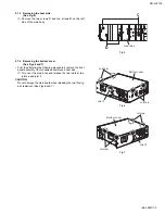
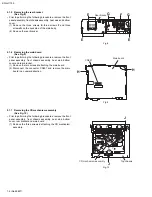
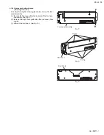
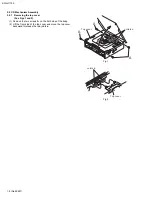
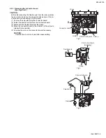
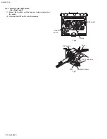
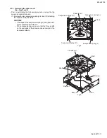
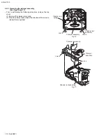
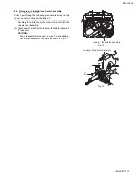
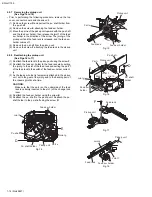
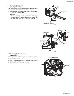
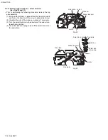
Disassembly method . . . . . . . . . . . . . . . . . . . . . . . . . . . . . . . . . . . . . . . . . . . . . . . . . . . . . . . . . . . . . . . . . . 1-4
3
Adjustment. . . . . . . . . . . . . . . . . . . . . . . . . . . . . . . . . . . . . . . . . . . . . . . . . . . . . . . . . . . . . . . . . . . . . . . . . . 1-23
4
Description of major ICs. . . . . . . . . . . . . . . . . . . . . . . . . . . . . . . . . . . . . . . . . . . . . . . . . . . . . . . . . . . . . . . 1-27
Area Suffix
U ----------- Otherr Areas
Summary of Contents for KD-LH1105
Page 47: ...KD LH1105 No 49827 1 47 ...