background image

SERVICE MANUAL

CD RECEIVER

No.49537

Feb. 2000

COPYRIGHT      2000 VICTOR COMPANY OF JAPAN, LTD.

This service manual is made from 100% recycled paper.

Printed in Japan
200002(O)

VICTOR COMPANY OF JAPAN, LIMITED

MOBILE ELECTRONICS  DIVISION,10-1,1Chome,Ohwatari-machi,Maebashi-city,Japan

KD-LX10
KD-LX30

(No.49537)

KD-LX10/KD-LX30

KD-LX10/KD-LX30

Area Suffix

J ---- Nortern America

Contents

Safety precaution

1-2

Instructions

1-3~

Disassembly method

2-1

Adjustment method

2-4

Maintenance of laser pickup

2-14

Replacement of lase pickup

2-14

Extention code connecting method

2-15

Functions of the mechanism under
  the servise mode

2-18

Flow of functional until TOC read

2-20

Description of major ICs

2-23

Block diagrams

2-39

Standard schematic diagrams

2-41

Printed circuit board

2-45,46

Parts list

3-1~7

Summary of Contents for KD-LX10

Page 1: ...No 49537 KD LX10 KD LX30 KD LX10 KD LX30 Area Suffix J Nortern America Contents Safety precaution 1 2 Instructions 1 3 Disassembly method 2 1 Adjustment method 2 4 Maintenance of laser pickup 2 14 Replacement of lase pickup 2 14 Extention code connecting method 2 15 Functions of the mechanism under the servise mode 2 18 Flow of functional until TOC read 2 20 Description of major ICs 2 23 Block dia...

Page 2: ...r on some parts of the chassis Therefore pay attention to such burrs in the case of preforming repair of this system Safety precaution CAUTION Please use enough caution not to see the beam directly or touch it in case of an adjustment or operation check ...

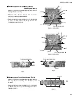
Page 3: ... body Remove the two screws E and the screw F on the back of the body Remove the two screws G on the upper side of the body Move the top chassis upward and disconnect the CD mechanism connector from the main board connector by pulling it Remove the top chassis from the body 1 2 3 4 5 6 Disassembly method Removing the top chassis See Fig 1 to 5 Fig 1 Fig 2 Fig 3 Fig 4 1 KD LX30 Fig 4 2 KD LX10 Fig ...

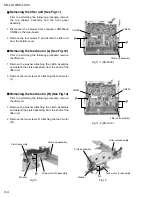
Page 4: ...ed with the rear panel and the rear heat sink Remove the screw J and the two screws K attaching the rear heat sink on the back of the body Remove the two screws L and the screw M attaching the rear panel Now the main board assembly will be removed 1 2 3 4 5 Removing the main board assembly See Fig 6 and 7 when reassembling correctly engage the switch S561 and S562 on the main board with the part e...

Page 5: ...y See Fig 6 8 and 9 Prior to performing the following procedure remove the top chassis assembly and the front panel assembly Remove the four screws O attaching the front board on the back of the front panel assembly and release the eight joints b 1 Removing the Front Board See Fig 10 Fig 6 1 KD LX30 Fig 6 2 KD LX10 Fig 8 Fig 9 Fig 10 H CN504 CN701 Front panel assembly CN702 CN503 H H CN504 CN701 F...

Page 6: ... from the shaft of the lifter unit Remove the two screws Q attaching the feed motor L 1 2 Removing the feed motor L See Fig 12 Prior to performing the following procedure remove the lifter unit Remove the washer attaching the clutch assembly and detach the clutch assembly from the shaft of the lifter unit Remove the two screws R attaching the feed motor R 1 2 Removing the feed motor R See Fig 13 C...

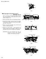
Page 7: ...n assembly Disconnect the card wire from connector CN702 on the main board and remove the operation assembly 1 2 3 Removing the operation assembly See Fig 14 to 17 when reassembling correctly engage the switch S561 and S562 on the main board and the right gear with the part e of the operation assembly ATTENTION Fig 14 Fig 15 Fig 16 Fig 17 S Spring 6 CN702 Operation assembly Spring 5 S Operation as...

Page 8: ...switch board from inside of the button panel 1 2 Removing the operation switch board See Fig 18 and 19 Prior to performing the following procedure remove the top chassis Remove the three screws U and the CD mechanism assembly from the top chassis 1 Removing the CD mechanism assembly See Fig 20 Button panel Operation switch board Button panel CD mechanism assembly Fig 18 Fig 19 Fig 20 T T U U U ...

Page 9: ...m control board Remove the CD mechanism control board in the direction of the arrow while releasing it from the two damper bracket slots i and the front bracket slot j Disconnect the flexible wire from connector on the pickup unit Removing the CD mechanism control board See Fig 1 and 2 Turn the FD gear in the direction of the arrow to move the entire pickup unit to the appropriate position where t...

Page 10: ... the three screws I and the damper bracket Raise the both sides fix arms and move the fix plates in the direction of the arrow to place the four shafts l as shown in Fig 8 and 9 Remove the CD mechanism ass y and the two springs m attaching the flame Remove the two screws J and both sides rear damper brackets from the dampers Detach the CD mechanism ass y from the left side to the right side 1 2 3 ...

Page 11: ...ach the FD gear part of the pickup unit upward Then remove the pickup unit while pulling out the part n of the FD screw 1 Remove the screw L attaching the nut push spring plate and the pickup mount nut from the pickup unit Pull out the FD screw 2 Removing the pickup unit See Fig 10 and 11 When reattaching the pickup unit reattach the part o of the pickup unit then the part n of the FD screw ATTENT...

Page 12: ...acket slot e Disconnect the flexible wire from connector on the pickup unit Removing the CD mechanism control board See Fig 1 and 2 Turn the FD gear in the direction of the arrow to move the entire pickup unit to the appropriate position where the flexible wire of the CD mechanism unit can be disconnected easily Refer to Fig 2 ATTENTION Fig 1 Fig 2 Fig 3 Fig 4 Front bracket CD mechanism control bo...

Page 13: ... Raise the both sides fix arms and move the fix plates in the direction of the arrow to place the four shafts g as shown in Fig 8 and 9 Remove the CD mechanism ass y and the two springs h attaching the flame Remove the two screws E and both sides rear damper brackets from the dampers Detach the CD mechanism ass y from the left side to the right side 1 2 3 4 Removing the CD mechanism ass y See Fig ...

Page 14: ...ickup mount nut from the pickup unit Pull out the FD screw 2 Removing the pickup unit See Fig 10 and 11 When reattaching the pickup unit reattach the part k of the pickup unit then the part j of the FD screw ATTENTION Prior to performing the following procedure remove the CD mechanism control board the front bracket loading motor the CD mechanism ass y and the feed motor ass y Turn up the CD mecha...

Page 15: ...KD LX10 KD LX30 2 13 ...

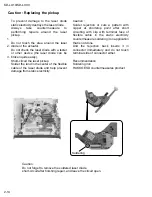
Page 16: ... of the flexible cable of the laser diode and help prevent damage from static electricity Caution Solder rejection or cuts a pattern with nipper at shortstop point after short circuiting with clip with terminal face of flexible cable in the static electricity countermeasure soldering iron application that is not done And the rejection back inserts it in connector immediately and do not touch termi...

Page 17: ...Since this adjustment should be performed to match the characteristics of the whole optical block do not touch the semi fixed resistor If the laser power is lower than the specified value the laser diode is almost worn out and the laser pickup should be replaced If the semi fixed resistor is adjusted while the pickup is functioning normally the laser pickup may be damaged due to excessive current ...

Page 18: ...n the main board Using the 2pin extention cord EXTLX001 2p connect the harness of the feed motor R assembly with the connector CN504 on the main board Extension code connecting method 1 2 Using the jig board EXTLX002 SWPWB its installing to the chassis then using 4pin extention cord EXTLX002 4P connect the harness of the lifter detecting board with the connector CN704 on the board Connect the conn...

Page 19: ...6Pin 30cm flat wire 6Pin x 2 interlocking connector 16Pin flat wire 16Pin interlocking connector 3 switch PWB 4Pin 30cm extension cord EXTLX001 2P EXTLX001 6PF EXTLX001 6PC EXTLX002 16PF EXTLX002 16PC EXTLX002 SWPWB EXTLX002 4P No Parts number Quantity Description Besides the above kit we offer the conventional extension cord for CD mechanism which are not essential to operation check or service T...

Page 20: ...KD LX10 KD LX30 2 18 Reassembly 1 Perform reassembly be reversing the removing process of removal of main parts CAUTION 1 Prior to reattaching the heat sink make sure to reattache the top chassis ...

Page 21: ... from factry This mode is used only when the CD changer is connected This mode is used only when the CD changer is connected Running mode Do not use this mode under the servise mode Deletion of CD error code and RDS data Calling of CD mechanism error code With the three error modes stored in maximum in the internal memory of the mechanism in the body of this system it is posible under the service ...

Page 22: ... case of time over 0 6sec of timer TEXT data reading error 04 0051 04 0052 81 0053 82 0054 82 0055 84 0059 80 0060 80 0061 80 0062 80 0063 The pickup cannot returned to the inner peripheral and the REST switch is not turned off The pickup cannot be returned to the outer peripheral and the REST switch is not turned off In case the focus cannot be searched by one set of focus searching 3 way focus s...

Page 23: ... correctly emits Microprocessor commands Rough Servo Mode CLV Servo Mode ProgramArea CLV Servo Mode Lead In Area Digital 0 RF signal Flow of functional operation until TOC read When the pickup correctly moves to the inner area of the disc TERMINAL Microprocessor commands FMO MN662748RPM 32 FEED MOTOR TERMINAL IC661 26 REST SW When the disc correctly rotates Tracking Servo Loop ON Servo CLV Rough S...

Page 24: ... pins 17 20 Check the pickup and its connections NO YES YES YES Does the S search waveform appear at IC601 pins 17 and 18 Is the disk rotated Does the RF signal appear at TP1 Is 3 5V present at IC661 pins 1 and 2 Check the spindle motor and its wiring Is 4V present at IC631 pin 25 Check the vicinity of IC661 Check IC601 and IC631 YES NO NO NO NO NO YES YES YES Check the circuits in the vicinity of...

Page 25: ...7 reverse input CH7 motor speed control Stand by Power save All mute Power supply voltage CH7 drive output IN2 IN2 OUT2 IN3 IN3 OUT3 IN4 IN4 OUT4 CTL1 FWD1 REV1 CTL2 FWD2 REV2 SGND FWD3 REV3 CTL3 SB PS MUTE PVCC2 DO7 Pin No Symbol I O Function 25 26 27 28 29 30 31 32 33 34 35 36 37 38 39 40 41 42 43 44 45 46 47 48 O O O O O O O O O O O O O I O I I I I O CH7 drive output CH6 drive output CH6 drive ...

Page 26: ... BUS signal cut in input terminal Power save 2 CRUISE signal input terminal Non connect Non connect Remote control signal input terminal Power supply terminal Power supply terminal Connect to ground Connect to ground Key control 0 input terminal Key control 1 input terminal Key control 2 input terminal Level meter signal input terminal Non connect S meter level input terminal Connect to ground Woo...

Page 27: ...inal Data input terminal Non connect Amp cut off signal output terminal Connect to ground DIMMER signal input terminal Power save 1 Power ON OFF select signal output terminal Power supply control terminal for CD Mute signal output terminal Non connect Non connect Non connect Power supply terminal Data output terminal Clock signal output terminal Non connect Non connect LCD reset signal output term...

Page 28: ... 10 11 12 13 14 CL Vcc INL NFL FIL NFR INR CR CR RGND OUTR OUTL LGND CL Powe supply terminal for amp power supply terminal input terminal Negative feedback terminal Filter terminal Negative feedback terminal Input terminal Power supply terminal for amp Output terminal of internal amp Rch GND terminal Rch output terminal Lch output terminal Lch GND terminal Output terminal of internal amp Pin No Sy...

Page 29: ...C block This output voltage is approximately 0 7V lower than VDD S The max output current is 100mA Control of the COMP output by inputting voltage This output voltage is 5 7V and max output current is 100mA This voltage supply is for microcomputer Whenever back up voltage supply is connected the output keeps on running This output voltage is 9 0v and max output current is 500mA This voltage supply...

Page 30: ...ont output terminal CH1 bus filter setting terminal CH1 bus filter setting terminal CH2 bus filter setting terminal CH2 bus filter setting terminal CH2 treble filter setting terminal CH1 treble setting terminal CH2 treble input terminal CH2 BBE II signal output terminal CH2 output mix amp negative input terminal A2 B2 C2 D2 FIL GND SI SC VCC OUTR2 OUTF2 OUTR1 OUTF1 BOUT1 BNF1 BOUT2 BNF2 TNF2 TNF1 ...

Page 31: ...ircuit Power supply voltage det VCC GND A0 A1 A2 SCL SDA WP I I I O I Power supply GND No use connect to GND Serial clock input Serial data I O of slave and ward address Write protect terminal Symbol I O Function BR24C16F X IC703 EEPROM 1 Pin layout 3 Block diagram 2 Pin function 14 13 12 11 8 10 9 1 2 3 4 7 5 6 VDD C1 C4 I O4 I O3 O I4 O I3 I O1 O I1 O I2 I O2 Vss C2 C3 BU4066BCFV X IC322 Quad an...

Page 32: ...d Circuit 1 Sample as Load Circuit 1 Sample as Load Circuit 1 1k 1k S1 CL Inputs Outputs C L H H A X L H Y Z H L 1 2 3 4 5 6 7 14 13 12 11 10 9 8 HD74HC126FP X IC771 Buffer 1 Pin layout 3 Block diagram 2 Function A B 1 2 3 4 A OUTPUT A INPUT A INPUT V 8 7 6 5 V B OUTPUT B INPUT B INPUT NJM4565M W IC151 IC171 IC323 IC361 IC461 Ope amp ...

Page 33: ... Pin function 1 58 59 60 65 66 67 68 69 71 72 73 74 75 76 77 78 79 80 O O O O I O I I I I I O Segment driver output terminal Common driver output terminal Common driver output terminal Common driver output terminal Power supply for logic section Power supply for LCD driver section LCD voltage input terminal Connect to ground Oscillation output terminal Oscillation input terminal Reset signal input...

Page 34: ... data input Common driver output pins The frame frequency is given by t0 fosc 384 Hz Power supply connection Provide a voltage of between 4 5 and 6 0V Display turning off input pin INT L Vss off S1 to S52 COM1 to COM3 L INT H VDD on Serial data can be transferred in display off mode Used for applying the LCD drive 2 3 bias voltage externally Must be connected to VDD2 when a 1 2 bias drive scheme i...

Page 35: ... OUTPUT 1 A INPUT 2 A INPUT 3 V 4 8 V 7 B OUTPUT 6 B INPUT 5 B INPUT V OUTPUT V INPUT INPUT NJM2100M W IC821 Dual operation amplifier 1 Pin layout 2 Block diagram Vcc Vout GND 1 3 2 OP1 Co1 IC PST600M G W IC702 System reset ...

Page 36: ...D LX10 KD LX30 2 34 A OUT 1 A IN 2 A IN 3 GND 4 8 V 7 B OUT 6 B IN 5 B IN OUTPUT Q13 Q6 Q5 Q7 Q11 Q12 Q10 V Q1 Q2 Q3 Q4 INPUTS Q8 Q9 NJM2904M W IC951 Dual operation amplifier 1 Pin layout 2 Block diagram ...

Page 37: ... circuit RPM6938 SV4 IC603 Remote control receiver TDA7560 IC941 4ch bridge amplifier 1 Pin layout 2 Block diagram 25 1 HSD ST BY 4 MUTE 22 IN1 11 IN2 12 IN3 15 IN4 14 AC GND S GND SVR TAB 16 10 1 13 25 HSD 9 OUT1 7 OUT1 8 P GND1 5 OUT2 3 OUT2 4 P GND2 17 OUT3 19 OUT3 18 P GND3 21 OUT4 23 OUT4 22 P GND4 VCC1 VCC2 6 20 ...

Page 38: ...0k ohm 20k ohm 20k ohm 13k ohm 680 ohm 2 12k ohm BOTTOM PEAK 20k ohm 20k ohm 20k ohm 12k ohm 1 74k ohm 47k ohm 12k ohm 180k ohm 50uA 21k ohm 21k ohm 7 96k ohm 10k ohm 10k ohm 10k ohm 10k ohm 10pF 36pF 50k ohm 15k ohm 30k ohm 7 67k ohm 10k ohm 30k ohm 15k ohm 20uA 21k ohm 29k ohm 24k ohm 24k ohm 65uA 20pF 180k ohm 20pF 180k ohm 180k ohm 40pF 40pF I I I I SW3 SW2 SW1 1k ohm LCD 3 STATE DET 20pF TEO ...

Page 39: ...CE DI CK DOUT SR I 01 I 02 OUT1 OUT2 VDD2 Crystal oscillator pin Non connect Chip enable input Serial data input Clock input Serial data output Register control pin I O ports I O ports Non connect Non connect Single power supply for REF frequency block O I I I O O I O I O Pin No Symbol I O Function 13 14 15 16 17 18 19 20 21 22 23 24 IFC VDD FMIN AMIN DGND FMCP VT AMCP VCC RF AGND XIN IF signal in...

Page 40: ... sync signal output terminal Sub code block sync signal output terminal Processor status signal readout clock output terminal Processor status signal output terminal Correction frame clock output terminal 7 35kHz Internal signal DSP internal flag and PLL clock output terminal Digital power supply voltage terminal Test input output terminal Normally keep at L level PLL double reference voltage supp...

Page 41: ... flag output terminal for internal signal Digital power supply voltage terminal Digital GND terminal General I O terminal This terminal control IO0 IO3 terminal Normally keep at open DAC test mode terminal Normally keep at open Test input terminal Normally keep at L level Test input output terminal Normally keep at L level Digital GND terminal Crystal oscillator connecting input terminal for DSP C...

Page 42: ...KD LX10 KD LX30 2 40 ...

Page 43: ...CD DRIVER CB1 CB3 SB1 SB52 CA1 CA3 SA1 SA52 IC603 REMOCON CN601 CN631 KEY1 KEY2 INV LCDRST LCDCE1 LCDCL LCDDA REMOCON LCDRES LCDCE2 LCDCL LCDDF LED KEY0 KEY1 to CN701 to CN702 PICKUP OPTIMA720 FOCUS COIL TRACKING COIL M M M LOADING MOTOR FEED MOTOR SPINDLE MOTOR REST SWITCH SW1 SW4 CN501 LOADING REST SPINDLE FEED SW1 SW4 A B C LD FOCUS TRACKING IC581 CD TRAY DOOR DRIVER IC501 RF AMP VA VB VC MO LD...

Page 44: ...WITCH IC601 LCD DRIVER IC602 LCD DRIVER CB1 CB3 SB1 SB52 CA1 CA8 SA1 SA60 IC603 REMOCON CN601 CN631 KEY1 KEY2 INV LCDRST LCDCE1 LCDCL LCDDA REMOCON LCDRST LCDCE2 LCDCL LCDDA LED KEY0 KEY1 to CN701 to CN702 PICKUP OPTIMA720 FOCUS COIL TRACKING COIL M M M LOADING MOTOR FEED MOTOR SPINDLE MOTOR REST SWITCH SW1 SW4 CN501 LOADING REST SPINDLE FEED SW1 SW4 A B C LD FOCUS TRACKING IC581 CD TRAY DOOR DRIV...

Page 45: ...Standard schematic diagrams KD LX10J Main amp section FRONT SIGNAL REAR SIGNAL TUNER SIGNAL CD SIGNAL CD CHANGER SIGNAL ...

Page 46: ...CD SIGNAL KD LX10J CD servo LCD control section ...

Page 47: ...KD LX30J Main amp section AUX SIGNAL FRONT SIGNAL REAR SIGNAL TUNER SIGNAL CD SIGNAL CD CHANGER SIGNAL ...

Page 48: ...KD LX30J CD servo LCD control section CD SIGNAL ...

Page 49: ...Printed circuit boards KD LX10J Main board Forward side Main board Reverse side LCD board Forward side LCD board Reverse side Switch board Forward side Switch board Reverse side ...

Page 50: ...KD LX30J Main board Forward side Main board Reverse side LCD board Forward side LCD board Reverse side Switch board Forward side Switch board Reverse side ...

Page 51: ...re not available as service parts Contents Exploded view of general assembly and parts list CD mechanism assembly and parts list Electrical parts list Packing materials and accessories parts list KD LX10 KD LX30 3 3 3 5 3 8 3 14 Areas suffix J Northern America ...

Page 52: ...44 R244 C941 NRSA02J 823X NRSA02J 823X NRSA02J 823X NRSA02J 823X QERF1CM 106Z NRSA02J 473X NRSA02J 473X NRSA02J 473X NRSA02J 473X QEKJ1HM 474Z MG RESISTOR MG RESISTOR MG RESISTOR MG RESISTOR E CAPACITOR 6 11 12 81 104 LV31602 003A LV41200 003A LV41200 003A LV30946 005A LV41863 001A LV31602 001A QYSDST2612Z QYSDST2610Z LV30946 003A LV41572 001A SIDE HEAT SINK SCREW FOR IC SCREW REAR HEAT SINK POWER...

Page 53: ...0 91 93 74 74 75 14 34 31 38 24 48 48 27 26 44 54 54 42 54 55 45 53 64 60 62 64 64 64 53 28 43 46 57 39 55 54 54 54 41 40 46 25 53 37 32 33 35 26 27 48 50 29 22 19 19 20 18 13 13 13 77 76 77 30 21 50 52 15 23 7 36 103 107 105 106 104 17 17 17 83 87 85 85 81 80 87 87 97 96 96 83 82 13 12 79 79 84 79 79 99 99 63 61 59 58 65 Switch board Main board LCD board ...

Page 54: ...N BASE BKT 1 22 LV41500 001A BUTTON B SUPORT 1 23 LV41545 001A BUTTON B GUIDE 1 24 LV31609 001A FRONT BKT ASS Y 1 25 LV20614 001A LOADING BKT ASS 1 26 WDM215025 WASHER 4 27 LV41503 001A ARM 3 2 28 LV31777 001A FFC GUIDE 1 29 LV31610 001A ROD GEAR 1 30 LV31604 001A BOTTOM ASS Y 1 31 QAR0029 001 FEED MOTOR 1 FOR BKT MOTOR L 32 PPN 13KA10C MOTOR 1 FOR BKT MOTOR R 33 LV40847 002A SPACER 1 MOTOR R 34 W...

Page 55: ...1 74 VKZ4777 001 MINI SCREW 4 D PANEL SW PWB 75 WJT0031 001A E CARD WIRE 1 76 LV31617 001A NAME PLATE 1 KD LX10 LV31660 001A NAME PLATE 1 KD LX30 77 LV41143 001A SHEET 2 79 GE40101 001A PIN CAP 2 KD LX10 GE40101 001A PIN CAP 8 KD LX30 80 LV30943 005A S REAR BRACKET 1 81 LV30946 003A REAR HEAT SINK 1 82 LV40790 001A PIN CORD BRKT 1 83 QYSDST2604Z SCREW 2 84 QYSDST2612Z SCREW 2 85 QYSDSP2606Z SCREW ...

Page 56: ...0 41 42 47 46 103 30 49 49 31 d 112 55 56 47 107 131 36 107 107 d 38 32 54 34 33 130 106 29 108 106 46 135 104 107 40 63 39 a 51 132 35 37 86 113 113 134 87 80 117 92 84 54 78 c 79 88 93 22 22 89 62 81 82 85 83 114 115 116 102 101 108 100 133 57 CD mechanism assembly and parts list Block No M M M 2 Grease G 31SA G 31SA Bottom side RX 405 TN CCD1001Z 138 ...

Page 57: ... 30310125T S L ARM SPRING 1 20 30310149T REAR DAM BKT Z 1 22 30310151T HUNG UP SP FZ 2 23 30310129T HUNG UP SP R 2 29 30300510T PU GEAR B 1 30 T T BASE Z 1 31 TURN TABLE Z 1 32 30310544T F M BASE Z 1 33 30310547T FD GR BLK Z 1 34 FD GR AZ 1 35 FD GR CZ 1 36 30310546T PU GUIDE Z 1 37 FD SCREW Z 1 38 30310533T THRUST SPR M 1 39 30310548T PU M NUT Z 1 40 30310512T NUT PUSH SPR PL 1 41 30310558T CLP A...

Page 58: ...311124T SW ACTUATOR 1 92 30311129T LDG BELT 1 93 30311140T FRONT BRKT J 1 100 9C0620503T C B TAP SCREW 2 M2X5 101 9C2020401T C SCREW TS G 5 M2X4 102 9C4320403T C B TAP SCREW 4 M2X4 103 9C0117223T SCREW 2 M1 7X2 2 104 9C4217703T C TAP SCREW S3 1 M1 7X7 105 9C0320201T C TAP SCREW S3 1 M2X2 106 9C4920013T C TAP SCREW S3 2 M2X10 107 9C4920603T C TAP SCREW B3 4 M2X6 108 9P0220031T TAMS SCREW 2 M2X3 110...

Page 59: ...41CM 106 E CAPACITOR KD LX30 C 273 QERF0JM 226Z E CAPACITOR KD LX30 C 301 QEK41EM 475 E CAPACITOR KD LX30 C 302 QEK41EM 475 E CAPACITOR KD LX30 C 303 QEK41CM 476 E CAPACITOR KD LX30 C 304 QEKJ1AM 107Z E CAPACITOR KD LX10 C 305 QEK41EM 475 E CAPACITOR 4 7MF 20 25V C 306 QEK41EM 475 E CAPACITOR 4 7MF 20 25V C 307 QEKJ1AM 107Z E CAPACITOR KD LX30 C 308 QEK41EM 475 E CAPACITOR 4 7MF 20 25V C 309 QEK41...

Page 60: ... C CAPACITOR C 822 NCB21EK 393X C CAPACITOR C 823 NCB21EK 393X C CAPACITOR C 824 NCB21EK 393X C CAPACITOR C 825 NCB21EK 393X C CAPACITOR C 826 NCB21HK 122X C CAPACITOR C 827 QEK41CM 106 E CAPACITOR 10MF 20 16V C 828 QEKJ1CM 226Z E CAPACITOR 22MF 20 16V C 911 QEK41CM 476 E CAPACITOR 47MF 20 16V C 912 QEKJ1AM 107Z E CAPACITOR 100MF 20 10V C 913 NCB21HK 104X C CAPACITOR C 931 NDC21HJ 101X C CAPACITOR...

Page 61: ...N2211 X TRANSISTOR Q 983 2SD601A R X TRANSISTOR R 1 NRSA02J 0R0X MG RESISTOR R 4 NRSA02J 473X MG RESISTOR R 5 NRSA02J 332X MG RESISTOR R 6 NRS181J 8R2X MG RESISTOR R 7 NRSA02J 473X MG RESISTOR R 8 NRSA02J 472X MG RESISTOR R 9 NRSA02J 473X MG RESISTOR R 10 NRSA02J 103X MG RESISTOR R 18 NRSA02J 223X MG RESISTOR R 21 NRSA02J 0R0X MG RESISTOR R 22 NRSA02J 622X MG RESISTOR R 23 NRSA02J 222X MG RESISTOR...

Page 62: ...A02J 103X MG RESISTOR KD LX10 R 364 NRSA02J 104X MG RESISTOR KD LX10 R 365 NRSA02J 153X MG RESISTOR KD LX10 R 366 NRSA02J 103X MG RESISTOR KD LX10 R 367 NRSA02J 471X MG RESISTOR KD LX10 R 401 NRSA02J 223X MG RESISTOR KD LX30 R 402 NRSA02J 223X MG RESISTOR KD LX30 R 403 NRSA02J 333X MG RESISTOR KD LX30 R 404 NRSA02J 333X MG RESISTOR KD LX30 R 405 NRSA02J 154X MG RESISTOR KD LX30 R 451 NRSA02J 224X ...

Page 63: ...SISTOR R 774 NRSA02J 101X MG RESISTOR R 775 NRSA02J 103X MG RESISTOR R 776 NRSA02J 104X MG RESISTOR R 777 NRSA02J 223X MG RESISTOR R 778 NRSA02J 101X MG RESISTOR R 779 NRSA02J 473X MG RESISTOR R 781 NRSA02J 331X MG RESISTOR R 782 NRSA02J 104X MG RESISTOR R 791 NRSA02J 102X MG RESISTOR R 821 QRE142J 102X C RESISTOR 1 0K 5 1 4W R 822 NRSA02J 822X MG RESISTOR R 823 NRSA02J 223X MG RESISTOR R 824 NRSA...

Page 64: ... MG RESISTOR R 613 NRSA02J 681X MG RESISTOR R 621 NRSA02J 221X MG RESISTOR R 622 NRSA02J 221X MG RESISTOR R 623 NRSA02J 821X MG RESISTOR R 624 NRSA02J 821X MG RESISTOR R 625 NRSA02J 471X MG RESISTOR R 626 NRSA02J 103X MG RESISTOR R 627 NRSA02J 221X MG RESISTOR R 628 NRSA02J 0R0X MG RESISTOR R 629 NRSA02J 102X MG RESISTOR R 630 NRSA02J 102X MG RESISTOR R 632 NRSA02J 221X MG RESISTOR R 633 NRSA02J 2...

Page 65: ...A1 A2 A5 Packing materials and accessories parts list Block No M M M 3 Block No M M M 4 A22 A3 A4 A6 A8 A19 A21 KIT1 A9 A13 Front view A23 ...

Page 66: ...CE NETWORK 1 KD LX10 BT 20071B SERVICE NETWORK 1 KD LX30 A 4 LVT0326 001C TROUBLE SHOOTIN 1 A 5 LVT0436 001A CAUTION SHEET 1 A 6 LVT0334 001A CAUTION SHEET 1 A 7 BT 51018 2 WARRANTY CARD 1 A 8 BT 51020 2 J REGIST CARD 1 A 9 VKZ4027 202 PLUG NUT 1 A 10 VKH4871 001 MOUNT BOLT 1 A 11 VKZ4328 001 LOCK NUT 1 A 12 WNS5000Z WASHER 1 A 13 FSKL4010 002 HOOK 2 A 14 RM RK31 REMOCON 1 A 15 QAB0014 001 BATTERY...

Reviews: