background image

SERVICE MANUAL

CD RECEIVER

No.49715

Jun. 2002

COPYRIGHT      2002 VICTOR COMPANY OF JAPAN, LTD.

KD-LX333R

KD-LX333R

Area Suffix            

E
EX

Continental Europe

Central Europe

Contents

Safety precaution

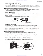
Preventing static electricity

Disassembly method

Adjustment method

1-2 

1-3 

1-4 

1-13

1-14

1-16

1-16

1-17~33

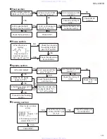
Flow of finctional operation intil opelation

   until 

TOC 

read

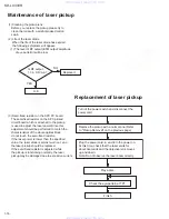
Maintenance of laser pickup

Replacement of laser pickup

Description of Major ICs

KD-LX333R

10

7

8

9

11

12

OFF

S

T

D

M

 ATT

SOURCE

www. xiaoyu163. com

QQ 376315150

9

9

2

8

9

4

2

9

8

TEL 13942296513

9

9

2

8

9

4

2

9

8

0

5

1

5

1

3

6

7

3

Q

Q

TEL  13942296513  QQ  376315150  892498299 

TEL  13942296513  QQ  376315150  892498299 

http://www.xiaoyu163.com

http://www.xiaoyu163.com

Summary of Contents for KD-LX333R

Page 1: ... 2 1 3 1 4 1 13 1 14 1 16 1 16 1 17 33 Flow of finctional operation intil opelation until TOC read Maintenance of laser pickup Replacement of laser pickup Description of Major ICs KD LX333R 10 7 8 9 11 12 OFF S T D M ATT SOURCE www xiaoyu163 com QQ376315150 9 9 2 8 9 4 2 9 8 TEL 13942296513 9 9 2 8 9 4 2 9 8 0 5 1 5 1 3 6 7 3 Q Q TEL 13942296513 QQ 376315150 892498299 TEL 13942296513 QQ 376315150 ...

Page 2: ...is system Safety precaution Please use enough caution not to see the beam directly or touch it in case of an adjustment or operation check www xiaoyu163 com QQ376315150 9 9 2 8 9 4 2 9 8 TEL 13942296513 9 9 2 8 9 4 2 9 8 0 5 1 5 1 3 6 7 3 Q Q TEL 13942296513 QQ 376315150 892498299 TEL 13942296513 QQ 376315150 892498299 http www xiaoyu163 com http www xiaoyu163 com ...

Page 3: ...Refer to the text 2 Do not use a tester to check the condition of the laser diode in the optical pickup The tester s internal power source can easily destroy the laser diode Handling the traverse unit optical pickup 1 Do not subject the traverse unit optical pickup to strong shocks as it is a sensitive complex unit 2 Cut off the shorted part of the flexible cable using nippers etc after replacing ...

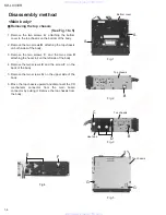
Page 4: ...side of the body Move the top chassis upward and disconnect the CD mechanism connector from the main board connector by pulling it Remove the top chassis from the body 1 2 3 4 5 6 Disassembly method Removing the top chassis See Fig 1 to 5 Main body Fig 1 Fig 2 Fig 3 Fig 4 Fig 5 Bottom cover A A B Top chassis Top chassis Heat sink C B E F Top chassis G G D www xiaoyu163 com QQ376315150 9 9 2 8 9 4 ...

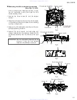
Page 5: ... procedure remove the top chassis assembly and the front panel assembly Remove the four screws I attaching the front board on the back of the front panel assembly and release the eight joints a 1 Removing the Front Board See Fig 9 Fig 6 Fig 8 Fig 7 Fig 9 Front panel assembly Front panel assembly H H Front panel assembly I I Joints a Joints a CN701 CN701 www xiaoyu163 com QQ376315150 9 9 2 8 9 4 2 ...

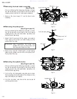
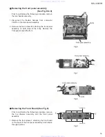
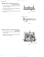
Page 6: ... 1 2 Removing the feed motor L See Fig 11 Prior to performing the following procedure remove the lifter unit Remove the washer attaching the clutch assembly and detach the clutch assembly from the shaft of the lifter unit Remove the two screws L attaching the feed motor R 1 2 Removing the feed motor R See Fig 12 Clutch assembly Fig 10 J Lifter unit assembly CN504 CN503 J Fig 11 Fig 12 Lifter unit ...

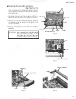
Page 7: ... Removing the operation assembly See Fig 13 to 16 When reassembling correctly engage the switch S651 and S652 on the main board and the right gear with the part b of the operation assembly ATTENTION Fig 13 Fig 14 Fig 15 Fig 16 M Spring 6 CN702 Operation assembly Spring 5 M Operation assembly b S652 S651 Operation assembly b Operation assembly b S652 S651 Bracket L Bracket R Bracket R www xiaoyu163...

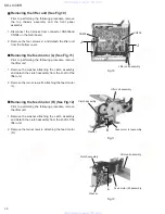
Page 8: ...rming the following procedure remove the top chassis Remove the three screws O and the CD mechanism assembly from the top chassis 1 Removing the CD mechanism assembly See Fig 19 Button panel Operation switch board Button panel CD mechanism assembly Fig 17 Fig 18 Fig 19 N N O O O www xiaoyu163 com QQ376315150 9 9 2 8 9 4 2 9 8 TEL 13942296513 9 9 2 8 9 4 2 9 8 0 5 1 5 1 3 6 7 3 Q Q TEL 13942296513 ...

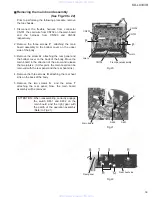
Page 9: ...nk Remove the three screws R attaching the rear heat sink on the back of the body Remove the two screws S and the screw T attaching the rear panel Now the main board assembly will be removed 1 2 3 4 5 Removing the main board assembly See Fig 20 to 22 When reassembling correctly engage the switch S651 and S652 on the main board and the right gear with the part b of the operation assembly Refer to F...

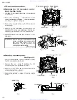
Page 10: ...y Refer to Fig 2 ATTENTION Prior to performing the following procedure remove the CD mechanism control board Remove the two springs f attaching the CD mechanism assembly and the front bracket Remove the two screws B and the front bracket while pulling the flame outward Remove the belt and the screw C from the loading motor 1 2 3 Removing the loading motor See Fig 3 to 5 CD mechanism section Fig 2 ...

Page 11: ... side to the right side 1 2 3 4 Removing the CD mechanism assembly See Fig 1 6 to 9 The CD mechanism assembly can be removed if only the rear damper bracket on the left side is removed ATTENTION Fig 6 Fig 7 Fig 8 Fig 9 Rear damper bracket Fix arm R Damper D D Damper bracket CD mechanism assembly Flame h h D D Fig 5 Front bracket CD mechanism control board Damper bracket h c d b a D D D CD mechanis...

Page 12: ...ching the pickup unit reattach the part j of the pickup unit then the part i of the FD screw ATTENTION Prior to performing the following procedure remove the CD mechanism control board the front bracket loading motor the CD mechanism assembly and the feed motor assembly Turn up the CD mechanism assembly and remove the two springs k on both sides of the clamper arms Open the clamper arm upward Turn...

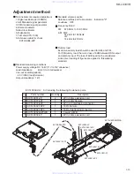
Page 13: ...considered since direct reading of figures are applied in this working o standard EXTGS004 22P Frequency Band FM 87 5 MHz to 108 0 MHz AM MW LW 522 kHz to 1620 kHz 144 kHz to 279 kHz EXTGS004 26P EXTLX001 2P EXTLX001 6PC EXTLX001 6PF EXTLX001 16PF EXTLX002 4P EXTLX002 SWPWB EXTLX002 16PC EXTLX001 2P EXTLX002 JIG Kit including the following 8 extension parts 1 2 3 4 5 6 7 2 1 1 1 1 1 1 2Pin 30cm ex...

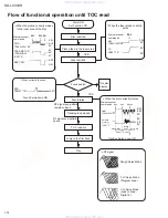
Page 14: ...r commands SEL TC94A14FA 38 LD CN501 15 No disc display When the disc correctly rotates Microprocessor commands DMO TC94A14FA 41 Spindle motor IC501 7 Tracking Servo Loop ON RF signal Rough Servo Mode v CLV Servo Mode Program Area CLV Servo Mode Lead In Area Digital 0 Flow of functional operation until TOC read 83 82 81 0V 6V 4V 2V OFF ON 3 3V Hi Z FEO TA2157 15 2 2V 84 3 3V 0V 4V 0V 84 86 A200 3 ...

Page 15: ... 8 9 and 15 Check the pickup and its connections Is the disk rotated Does the RF signal appear at TP1 Is the RF waveform at TP1 distorted Proceed to the Tracking section Is 4V present at IC501 pins 6 and 7 Check the spindle motor and its wiring Check the circuits in the vicinity of IC521 19 24 or the pickup Is 4V present at IC541 pins 41 Check IC541 and IC521 Check the vicinity of IC501 When the d...

Page 16: ...alue the laser diode is almost worn out and the laser pickup should be replaced If the semi fixed resistor is adjusted while the pickup is functioning normally the laser pickup may be damaged due to excessive current Is RF output 1 3 0 4Vp p YES NO O K Replace it Replacement of laser pickup Turn of the power switch and disconnect the power cord Replace the pickup with a normal one Refer to Pickup ...

Page 17: ... 28 29 30 31 32 64 63 62 61 60 59 58 57 56 55 54 53 52 51 50 49 BCK LRCK AOUT DOUT IPF V DD3 V SS3 SBOK CLCK DATA SFSY SBSY HSO UHSO PV DD3 PDO VXDD3 XO XI XV SS3 TEIN V DD3 V SS3 DMO FMO AV DD3 SEL TEBC RFGC V REF TRO FOO DVSS3 RO DVDD3 DVR LO DVSS3 ZDET VSS5 BUS0 BUS1 BUS2 BUS3 BUCK CCE RST VDD5 TEZI TEI SBAD FEI RFRP RFZI RFCT AVDD3 RFI SLCO AVSS3 VCOF RVREF LPFO LPFN TMAX TC9490FA IC521 DSP DA...

Page 18: ... PLL LPF amp PLL only VREF pin VCO filter pin Analog GND pin DAC output pin for data slice level generation RF signal input pin Zin selectable by command Analog 3 3V power supply voltage pin RFRP signal center level input pin RFRP signal zero cross input pin RF ripple signal input pin Focus error signal input pin Sub beam adder signal input pin Tracking error input pin Inputs when tracking servo i...

Page 19: ...A converter GND pin 1 bit DA converter zero data detection flag output pin Microcontroller interface GND pin Microcontroller interface data I O pins Microcontroller interface clock input pin Microcontroller interface chip enable signal input pin At L Bus0 to BUS3 are active Reset signal input pin At reset L Microcontroller interface 5V power supply pin Symbol RFGC TEBC SEL AVDD3 FMO DMO VSS3 VDD3 ...

Page 20: ...SW VRO FEO FEN RFRP RFRPIN RFGO RFGC AGCIN RFO RFN GND 14 15 16 17 18 19 20 21 22 23 24 12 RFDC TEO TEN TEBC SEL LDO MDI TNI TPI FPI FNI Vcc 11 10 9 8 7 6 5 4 3 2 1 TA2147F X IC501 RF amp 1 Terminal layout 2 Block diagram www xiaoyu163 com QQ376315150 9 9 2 8 9 4 2 9 8 TEL 13942296513 9 9 2 8 9 4 2 9 8 0 5 1 5 1 3 6 7 3 Q Q TEL 13942296513 QQ 376315150 892498299 TEL 13942296513 QQ 376315150 892498...

Page 21: ...al generation amp negative phase input pin Signal amp output pin for track count Combining RFRP signal TEO signal with TC9490F FA configures tracking search system Signal generation amp input pin for track count RF signal amplitude adjustment amp output pin RF amplitude adjustment control signal input pin Adjusts RF signal amplitude by eliminating carrier component from PWM signal 3 state output P...

Page 22: ... Protective circuit Mute circuit Ripple Filter Stand by Switch AC CONT2 0 22 F 2200 F 0 022 F 0 22 F AC CONT1 5V ST ON 47 F 0 22 F 0 22 F 22 F Mute 10K 3 3 F OUTLF OUTLF Low Level Mute ON GND OUTLR OUT LR GND 1 Block diagram www xiaoyu163 com QQ376315150 9 9 2 8 9 4 2 9 8 TEL 13942296513 9 9 2 8 9 4 2 9 8 0 5 1 5 1 3 6 7 3 Q Q TEL 13942296513 QQ 376315150 892498299 TEL 13942296513 QQ 376315150 892...

Page 23: ...r Rear Rch Power input Output for Front Rch Power GND Output for Front Rch Ripple filter Front Rch input Rear Rch input Signal GND Rear Lch input Front Lch input Power on time control Output for Front Lch Power GND Output for Front Lch Power input Output for Rear Lch Muting control input Output for Rear Lch Power GND Header of IC www xiaoyu163 com QQ376315150 9 9 2 8 9 4 2 9 8 TEL 13942296513 9 9 ...

Page 24: ...put STOP Pulse signal for CRUISE input only in 330R RDS clock input RDS data input Remocon input 111R READY 5V 5V Temperature detection input Key input 0 Key input 1 Key input 2 Level meter input MRC output voltage detection S QUALITY level input S METER level input GND Subwoofer volume control analog output Dot matrix contrast adjustment analog output 5V J BUS data input J BUS data output J BUS c...

Page 25: ... output IC control clock output IC control data input Telephone mute detection input POWER AMP ON OFF selection output GND Dimmer detection input L dimmer ON Power save 1 Operating together with ACC Power save L Operating H Power ON OFF selection output Power ON H CD power supply control signal output CD H Mute output MUTEON L Subwoofer cut off frequency control output 1 Subwoofer cut off frequenc...

Page 26: ... 3 with CDLSI H not for 8cm DISC L for 8cm DISC Symbol BUSO BUS1 BUS2 BUS3 DISCSEL NC REFR REFL FILTER 8 9 10 11 12 13 14 1 2 3 4 5 6 7 INR NFR FIL NFL CL Vcc INL CL LGND OUTL OUTR RGND CR CR 1 7 8 3220 14 BA3220FV X IC301 IC401 Line out amp 1 Pin layout 2 Block diagram www xiaoyu163 com QQ376315150 9 9 2 8 9 4 2 9 8 TEL 13942296513 9 9 2 8 9 4 2 9 8 0 5 1 5 1 3 6 7 3 Q Q TEL 13942296513 QQ 376315...

Page 27: ...etting Pin CH2 Bass Filter Setting Pin CH2 Treble Filter Setting Pin CH1 Treble Filter Setting Pin CH2 Treble Input Pin CH2 BBE II Signal Output Pin CH2 Output MIX Amplifier Inverse Input Pin A2 B2 C2 D2 FIL GND SI SC VCC OUTR2 OUTF2 OUTR1 OUTF1 BOUT1 BNF1 BOUT2 BNF2 TNF2 TNF1 TIN2 BBOUT2 MIX2 Pin No Symbol Function 23 24 25 26 27 28 29 30 31 32 33 34 35 36 37 38 39 40 41 42 43 44 CH2 High Pass VC...

Page 28: ...l clock input Serial data I O of slave and word address Write protect terminal Symbol I O Function BR24C32F X IC703 EEPROM 1 Pin layout 3 Block diagram 2 Pin function 14 13 12 11 8 10 9 1 2 3 4 7 5 6 VDD C1 C4 I O4 I O3 O I4 O I3 I O1 O I1 O I2 I O2 Vss C2 C3 BU4066BCFV X IC322 Quad analog switch 1 Pin layout Block diagram www xiaoyu163 com QQ376315150 9 9 2 8 9 4 2 9 8 TEL 13942296513 9 9 2 8 9 4...

Page 29: ...og Power supply Digital Power supply 4 3 5 6 12 11 13 14 10 9 BU1923F IC51 RDS decoder 7 8 16 1 2 MUX Vref VDD1 VSS1 VDD2 VSS2 Xl X0 T1 T2 RDATA QUAL RCLK CMP VSS3 RPM6938 SV4 IC602 Remote sensor Vcc Vcc Comp AGC AMP PD Detector BPF fo trimming circuit I V conversion magnetic shield Rout GND 22k 1 Block diagram www xiaoyu163 com QQ376315150 9 9 2 8 9 4 2 9 8 TEL 13942296513 9 9 2 8 9 4 2 9 8 0 5 1...

Page 30: ...T2 IN3 IN3 OUT3 IN4 IN4 OUT4 CTL1 FWD1 REV1 CTL2 FWD2 REV2 SGND FWD3 REV3 CTL3 SB PS MUTE PVCC2 DO7 Pin No Symbol I O Function 25 26 27 28 29 30 31 32 33 34 35 36 37 38 39 40 41 42 43 44 45 46 47 48 O O O O O O O O O O O O O I O I I I I O CH7 drive output CH6 drive output CH6 drive output Power ground2 CH5 drive output CH5 drive output CH4 drive output CH4 drive output CH3 drive output CH3 drive o...

Page 31: ...ied to CTRL pin Output voltage is VCC 1 V when M or H level to CTRL pin and H level to ANT CTRL Connected to ACC Regular 5 7V Output voltage is 5V when M or H level applied to CTRL pin Output for ACC detector L ANT output OFF H ANT output ON Connected to VCC Low battery detect Output voltage is 9V when M or H level applied to CTRL pin L BIAS OFF M BIAS ON H CD ON Output voltage is 8V when H level ...

Page 32: ... amp negative input terminal Microphone amp output terminal Ground Non connection VCA input terminal VCA control terminal VCA output terminal Power supply Vcc 2 Amp IN Amp IN Amp OUT GND NC VCA IN Vc VCA OUT Vcc Pin No Symbol Function 6 7 5 8 B 2 1 3 4 A A OUT A IN A IN VEE VCC B OUT B IN B IN NJM2100M IC821 Operational amp www xiaoyu163 com QQ376315150 9 9 2 8 9 4 2 9 8 TEL 13942296513 9 9 2 8 9 ...

Page 33: ...power pin LCD driver bias 0 4 voltage L level power pin Power supply pin to connect to ground Oscillator pin Display off general purpose output port L fixed input pin Chip enable Synchronization clock Transfer data SEG1 SEG73 SEG74 SEG75 COM8 COM1 P1 P4 VDD VLCD VLCD0 VLCD1 VLCD2 VLCD3 VLCD4 VSS OSC LCD RESET CE CL DI No Symbol I O Function OSC VLCD VLCD0 VLCD1 VLCD2 VLCD3 VLCD4 VDD VSS P1 P4 COM1...

Page 34: ...UNIT 10 1 1Chome Ohwatari machi Maebashi city 371 8543 Japan No 49715 200206 www xiaoyu163 com QQ376315150 9 9 2 8 9 4 2 9 8 TEL 13942296513 9 9 2 8 9 4 2 9 8 0 5 1 5 1 3 6 7 3 Q Q TEL 13942296513 QQ 376315150 892498299 TEL 13942296513 QQ 376315150 892498299 http www xiaoyu163 com http www xiaoyu163 com ...
Page 35: ...circuit boards 2 1 2 2 2 3 4 CD ROM No SML200106 Area Suffix E EX Continental Europe Central Europe KD LX333R 10 7 8 9 11 12 OFF S T D M ATT SOURCE www xiaoyu163 com QQ376315150 9 9 2 8 9 4 2 9 8 TEL 13942296513 9 9 2 8 9 4 2 9 8 0 5 1 5 1 3 6 7 3 Q Q TEL 13942296513 QQ 376315150 892498299 TEL 13942296513 QQ 376315150 892498299 http www xiaoyu163 com http www xiaoyu163 com ...
Page 36: ...yu163 com QQ376315150 9 9 2 8 9 4 2 9 8 TEL 13942296513 9 9 2 8 9 4 2 9 8 0 5 1 5 1 3 6 7 3 Q Q TEL 13942296513 QQ 376315150 892498299 TEL 13942296513 QQ 376315150 892498299 http www xiaoyu163 com http www xiaoyu163 com ...
Page 37: ...REGULATOR VCC LCDDA LCDDL LCDCF1 LCDCE2 LCDRST RSET REMOCON KEY1 KEY2 CN701 CN601 CN702 KEY0 KEY1 CN631 CN704 CN503 CN504 CASW1 CASW2 CASW3 CD L CD R L CH R CH BUS0 BUS1 BYS2 BUS3 BUCK CCE RST FOO FRD DMO FMO SLE TEB RFDC RFBC TE RFBO RFRP FEO VA VB VC MD LC CN501 TR SP FE LO FO DOOR TRAY CD MECHA KEY0 KEY1 REMOCON IC603 REMOCON IC601 LCD DRIVER LCDRST LCDCE1 LCDCL LCDDA KEY SWITCH LED LCD KEY2 IN...

Page 38: ...GNAL KD LX333R KD LX333R A B C D E F G 1 2 3 4 5 2 2 Standard schematic diagram Main amp section w w w x i a o y u 1 6 3 c o m Q Q 3 7 6 3 1 5 1 5 0 9 9 2 8 9 4 2 9 8 T E L 1 3 9 4 2 2 9 6 5 1 3 9 9 2 8 9 4 2 9 8 0 5 1 5 1 3 6 7 3 Q Q TEL 13942296513 QQ 376315150 892498299 TEL 13942296513 QQ 376315150 892498299 http www xiaoyu163 com http www xiaoyu163 com ...
Page 39: ...970 D961 R132 C406 C962 R133 R134 C403 R979 C410 IC401 D1014 D1015 D1009 C409 C402 C401 C310 C408 C309 C301 C407 C308 R241 R243 C243 R243 R145 R246 C941 D1016 D1010 C242 C241 C144 D1002 C141 C944 C995 C992 D1007 D1001 D1003 D1004 D1005 D1006 C942 R941 C142 D1008 D1013 D1012 C993 D1011 C998 C994 C997 C996 C991 CN901 R821 CN302 CN301 L961 C961 C302 C307 C301 C305 CN503 R141 R143 R146 C945 Q943 IC941...

Page 40: ...8 C755 Q791 IC702 R702 R718 TH700 R727 C722 C721 R722 R723 R716 R715 R714 Q700 R700 R719 C582 R962 R963 Q982 Q977 Q979 R965 D963 D980 D332 Q967 R971 R970 D978 R276 R277 C336 R339 R274 R338 R272 R176 R172 C337 R175 R177 R171 R912 R236 Q232 R235 R135 R911 R451 R452 C455 C357 C457 R455 C359 C454 C354 C362 R173 R174 C174 C118 R354 R454 C351 C120 C253 R353 R358 C458 R458 R401 R305 R302 R301 R304 R303 R...

Page 41: ...yu163 com QQ376315150 9 9 2 8 9 4 2 9 8 TEL 13942296513 9 9 2 8 9 4 2 9 8 0 5 1 5 1 3 6 7 3 Q Q TEL 13942296513 QQ 376315150 892498299 TEL 13942296513 QQ 376315150 892498299 http www xiaoyu163 com http www xiaoyu163 com ...
Page 42: ...NIT 10 1 1Chome Ohwatari machi Maebashi city 371 8543 Japan No 49715SCH 200206 www xiaoyu163 com QQ376315150 9 9 2 8 9 4 2 9 8 TEL 13942296513 9 9 2 8 9 4 2 9 8 0 5 1 5 1 3 6 7 3 Q Q TEL 13942296513 QQ 376315150 892498299 TEL 13942296513 QQ 376315150 892498299 http www xiaoyu163 com http www xiaoyu163 com ...
Page 43: ...lock No MB Electrical parts list Block No 01 02 Packing materials and accessories parts list Block No M3 M5 KD LX333R 3 3 3 5 3 8 3 14 Area suffix E Continental Europe EX Central Europe www xiaoyu163 com QQ376315150 9 9 2 8 9 4 2 9 8 TEL 13942296513 9 9 2 8 9 4 2 9 8 0 5 1 5 1 3 6 7 3 Q Q TEL 13942296513 QQ 376315150 892498299 TEL 13942296513 QQ 376315150 892498299 http www xiaoyu163 com http www ...
Page 44: ...w xiaoyu163 com QQ376315150 9 9 2 8 9 4 2 9 8 TEL 13942296513 9 9 2 8 9 4 2 9 8 0 5 1 5 1 3 6 7 3 Q Q TEL 13942296513 QQ 376315150 892498299 TEL 13942296513 QQ 376315150 892498299 http www xiaoyu163 com http www xiaoyu163 com ...
Page 45: ...109 110 112 111 19 15 16 18 LCD1 80 80 84 82 83 79 81 80 107 143 100 106 101 90 80 89 80 88 82 86 100 52 93 95 153 143 97 99 153 145 4 6 6 8 12 7 144 3 5 14 40 2 12 13 40 40 1 37 38 39 140 138 146 51 140 139 141 141 44 41 144 150 150 144 144 33 151 152 156 w w w x i a o y u 1 6 3 c o m Q Q 3 7 6 3 1 5 1 5 0 9 9 2 8 9 4 2 9 8 T E L 1 3 9 4 2 2 9 6 5 1 3 9 9 2 8 9 4 2 9 8 0 5 1 5 1 3 6 7 3 Q Q TEL 1...

Page 46: ...013660 FEED MOTER 1 QAR0029 001 Item Parts number Parts name Area A Parts list General assembly Q ty Description Block No M1MM 95 KA2502011 2P CONECTOR ASSY 1 97 000013680 MOTOR 1 QAR0188 001 99 KA2502012 2P CONECTOR ASSY 1 100 XP2020P1C SCREW 4 101 DG3151000 PUSH LEVER ASSY 1 106 DG3058000 FFC GUIDE 1 107 DG4116010 SHEET FRONT BK 1 108 DG1140013 PANEL BUTTON 1 109 DG2141011 BUTTON FUNC 1 110 DG21...

Page 47: ...13 23 23 20 49 1 15 14 17 16 70 71 90 91 100 101 101 101 101 102 102 100 110 105 12 86 3 6 9 7 7 4 2 5 88 93 79 92 22 106 108 106 132 TN CCD1001Z 150S b a b d c c d d a CD mechanism assembly and parts list Block No M M M B www xiaoyu163 com QQ376315150 9 9 2 8 9 4 2 9 8 TEL 13942296513 9 9 2 8 9 4 2 9 8 0 5 1 5 1 3 6 7 3 Q Q TEL 13942296513 QQ 376315150 892498299 TEL 13942296513 QQ 376315150 89249...

Page 48: ...30310544T F M BASE Z 1 33 30310547T FD GR BLK Z 1 36 30310546T PU GUIDE Z 1 38 30310533T THRUST SPR M 1 39 30310577T PU M NUT Z S 1 40 30310512T NUT PUSH SPR PL 1 41 30310558T CLP ARM Z 1 42 30310514T CLP ARM SPRING 1 43 30310552T CLAMPER Z 1 44 30310541T 8CM STOPPER M 1 45 30310566T 8CM STOP SPP Z 1 48 30310557T CLAMPER PLATE Z 1 49 30310524T DAMPER J 3 50 30310525T CLP ARM SPR L 1 51 30310545T F...

Page 49: ...20403T C B TAP SCREW 4 M2X4 103 9C0117223T SCREW 2 M1 7X2 2 104 9C0917703T C TAP SCREW S3 1 M1 7X7 105 9C0320201T C TAP SCREW S3 1 M2X2 106 9C4920013T C TAP SCREW S3 2 M2X10 107 9C4920603T C TAP SCREW B3 4 M2X6 108 9P0220031T TAMS SCREW 2 M2X3 110 9C0420253 C TAP SCREW 1 M2X2 5 113 9W0330276 NW BLUE 2 2 9X5X0 3 116 9W0725030T LUMILAR W 1 2 3X9 8X0 25 117 9W0640030T WASHER 1 1 4X3 2X0 4 130 3031053...

Page 50: ...0 47 MF C251 CE4754468 E CAPACITOR 4 7 MF 25V C252 CY122623J C CAPACITOR 0 0012MF C253 CZ1216D2J C CAPACITOR 120 PF C254 CZ1016D2J C CAPACITOR 100PF C272 CE1063468 E CAPACITOR 10 MF 16V C273 CE2260468 E CAPACITOR 22 MF 6 3V C3 CY103623J C CAPACITOR 0 01 MF C301 CE4754468 E CAPACITOR 4 7 MF 25V C302 CE4754468 E CAPACITOR 4 7 MF 25V C303 CE4763468 E CAPACITOR 47 MF 16V C305 CE4754468 E CAPACITOR 4 7...

Page 51: ...23J C CAPACITOR 0 0022MF C722 CY222623J C CAPACITOR 0 0022MF C750 CY474122J C CAPACITOR 0 47 MF C755 CY473623J C CAPACITOR 0 047 MF C756 CY222623J C CAPACITOR 0 0022MF C771 CY473623J C CAPACITOR 0 047 MF C791 CE1046468 E CAPACITOR 0 1 MF 50V C821 CY183623J C CAPACITOR 0 018 MF C822 CY393623J C CAPACITOR 0 039MF C823 CY393623J C CAPACITOR 0 039MF C824 CY393623J C CAPACITOR 0 039 MF C825 CY393623J C...

Page 52: ...STOR DTC114EUA X Q702 TRA1576 QRS L A TRANSISTOR 2SA1576A QR X Q791 TRC114EUL A DIGI TRANSISTOR DTC114EUA X Q942 TRC114TUL A DIGI TRANSISTOR DTC114EUA X Q943 TRC114EUL A DIGI TRANSISTOR DTC114EUA X Q965 TRC114EUL A DIGI TRANSISTOR DTC114EUA X Q966 TRA1576 QRS L A TRANSISTOR 2SA1576A QRS Q967 TRC4081 QRS L TRANSISTOR 2SC4081 QR X Q977 TRA114EUL A DIGI TRANSISTOR DTA114EUA X Q979 TRA114EUL A DIGI TR...

Page 53: ...344 RK105JA0J C RESISTOR 1 10W 1 M R351 RK224JA0J COMP RESISTOR 1 10W 220K R352 RK224JA0J COMP RESISTOR 1 10W 220K R353 RK105JA0J C RESISTOR 1 10W 1 M R354 RK682JA0J C RESISTOR 1 10W 6 8 K R355 RK224JA0J COMP RESISTOR 1 10W 220K R358 RK332JA0J C RESISTOR 1 10W 3 3 K R401 RK243JA0J C RESISTOR 1 10W 24 K R402 RK243JA0J C RESISTOR 1 10W 24K R403 RK333JA0J COMP RESISTOR 1 10W 33 K R404 RK333JA0J COMP ...

Page 54: ...R762 RK222JA0J C RESISTOR 1 10W 2 2 K R763 RK222JA0J C RESISTOR 1 10W 2 2 K R764 RK222JA0J C RESISTOR 1 10W 2 2 K R765 RK222JA0J C RESISTOR 1 10W 2 2 K R766 RK473JA0J COMP RESISTOR 1 10W 47 K R772 RK473JA0J COMP RESISTOR 1 10W 47 K R773 RK223JA0J COMP RESISTOR 1 10W 22 K R775 RK103JA0J C RESISTOR 1 10W 10 K R776 RK104JA0J COMP RESISTOR 1 10W 100 K R777 RK223JA0J COMP RESISTOR 1 10W 22 K R779 RK473...

Page 55: ...JA0J C RESISTOR 1 10W 2 2 K R609 RK683JA0J C RESISTOR 1 10W 68 K R610 RK222JA0J C RESISTOR 1 10W 2 2 K R611 RK472JA0J C RESISTOR 1 10W 4 7 K R612 RK472JA0J C RESISTOR 1 10W 4 7 K R613 RK681JA0J C RESISTOR 1 10W 680 R620 RK102JA0J C RESISTOR 1 10W 1 K R621 RK271JA0J C RESISTOR 1 10W 270 R622 RK331JA0J C RESISTOR 1 10W 330 R623 RK821JA0J C RESISTOR 1 10W 820 R624 RK821JA0J C RESISTOR 1 10W 820 R625 ...

Page 56: ...2 A6 A7 A8 A9 A10 A3 A22 A23 A12 A13 A14 A15 A16 A17 A20 A11 A18 A21 P4 A5 P3 A1 A2 www xiaoyu163 com QQ376315150 9 9 2 8 9 4 2 9 8 TEL 13942296513 9 9 2 8 9 4 2 9 8 0 5 1 5 1 3 6 7 3 Q Q TEL 13942296513 QQ 376315150 892498299 TEL 13942296513 QQ 376315150 892498299 http www xiaoyu163 com http www xiaoyu163 com ...
Page 57: ...1 001SS A 8 YN5005000 LOCK NUT 1 VKZ4328 001 A 9 DG4109000 HOOK 2 FSKL4010 002 A 10 YWS050400 WASHER 1 WNS5000Z A 11 PIM171200 INSTRUCTION 1 ENG GER FRE DUT A 12 PIM171300 INSTRUCTION E 1 SPA ITA SWE RUS A 13 PIM171400 INSTALLATION 1 ENG GER FRE DUT A 14 PIM171500 INSTALLATION E 1 SPA ITA SWE RUS A 15 PTC004000 CAUTION SHEET 1 LV40978 001A A 16 PTC003900 CAUTION SHEET 1 A 17 PTC004400 CAUTION SHEE...

Reviews: