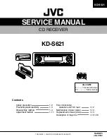
SERVICE MANUAL
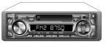
CD RECEIVER
No.49675
Jan. 2002
COPYRIGHT 2002 VICTOR COMPANY OF JAPAN, LTD.
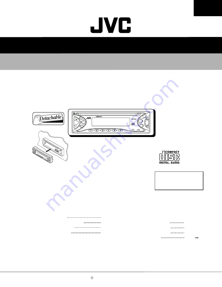
KD-S621
KD-S621
Contents
Safety precaution
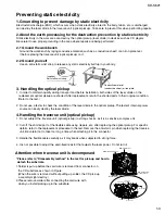
Preventing static electricity
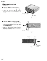
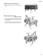
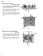
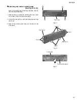
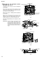
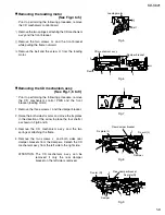
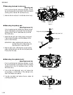
Disassembly method
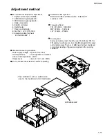
Adjustment method
1-2
1-3
1-4
1-11
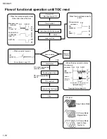
Flow of functional
operation unit TOC read
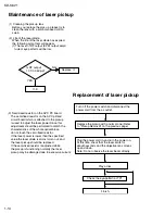
Maintenance of laser pickup
Replacement of laser pickup
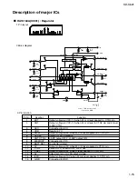
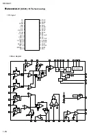
Description of major ICs
1-12
1-14
1-14
1-15 26
Area Suffix
E -------- Continental Europe
EX ------------ Central Europe
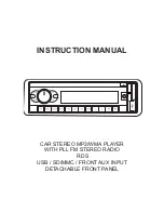
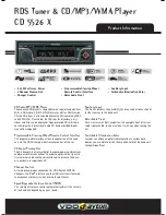
SEL
LOUD
DISP
SSM
¢
4
CD
FM
AM
SCM
MODE
7
8
9
10
11
12
RND
RPT
MO