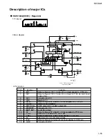
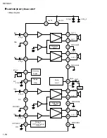
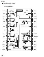

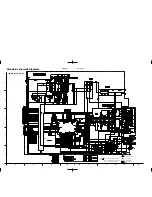
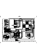


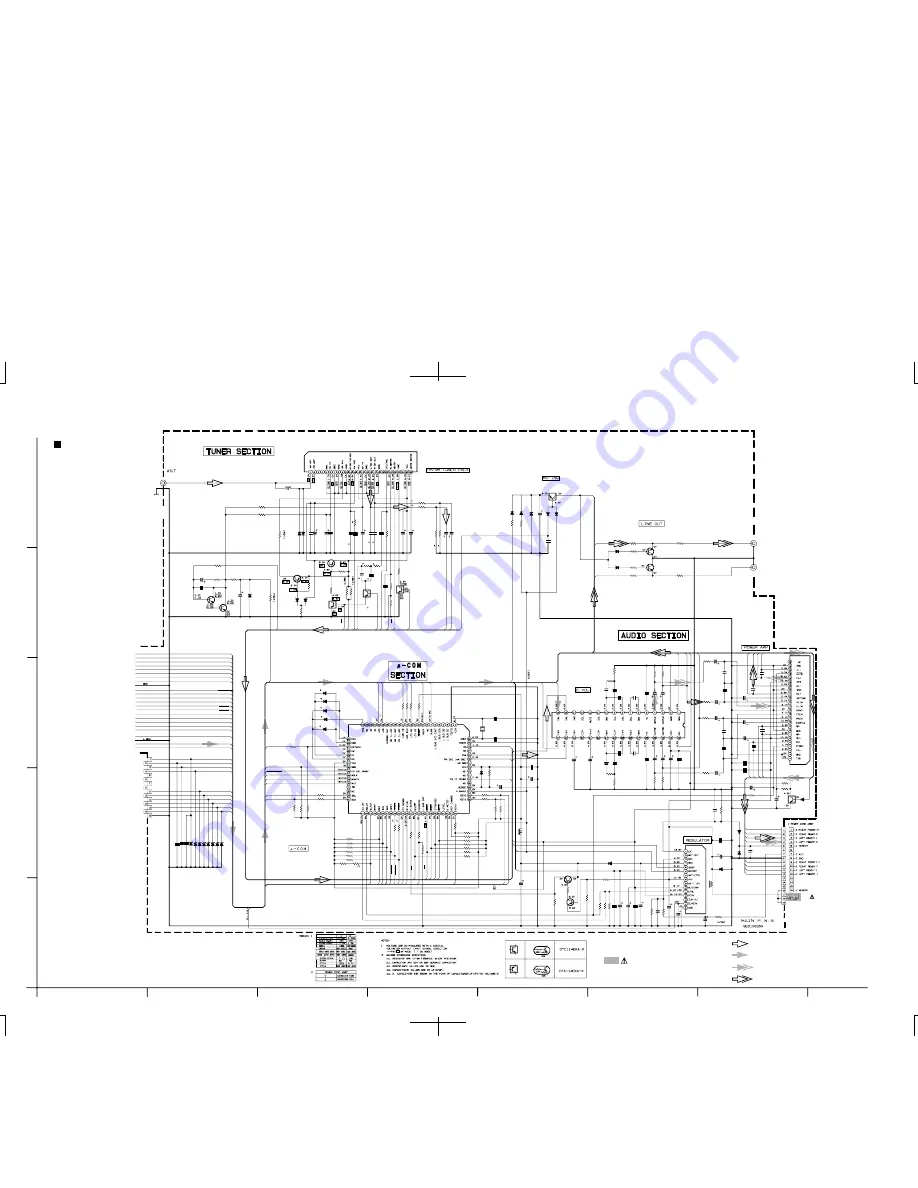
Tuner Signal
CD signal
Front signal
Rear signal
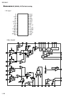
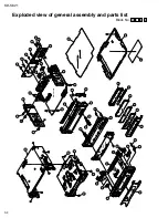
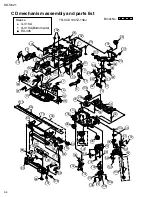
Parts are safety assurance parts.
When replacing those parts make
sure to use the specified one.
Main amp section
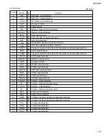
Standard schematic diagrams
H
A
B
C
D
E
F
G
1
2
3
4
5
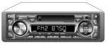
KD-S621
KD-S621
2-2
R828
R814
R815
R816
C803
C804
CJ701
R832
R834
R831
D804
C802
Q902
D903
C801
IC901
R907
R827
R811
R704
R823
R702
R808
R826
R825
C328
C331
C330
C329
R323
R807
D321
C405
C305
C404
C304
R401
R301
Q321
R307
R308
R408
R407
Q792
R333
IC801
R812
R840
R841
R842
C321
C327
R321
D332
D333
R322
C902
Q432
Q332
R845
R336
R433
L701
CN801
R201
R101
R703
TU701
R436
R434
IC321
D802
D805
D803
C334
C335
C332
F1
C333
C433
C432
C435
C434
C427
R902
C916
IC301
Q861
Q791
R791
Q732
Q731
C731
C732
R732
R733
R731
R701
C901
D901
R334
R829
D801
C807
D902
C904
D867
R862
D822
C717
R822
X801
D904
C720
R833
R835
C862
R796
D791
Q702
C718
R906
R910
C712
R798
R911
R909
R803
R904
R905
R901
R903
C903
C319
R817
L801
R801
C906
C909
C910
CJ321
R830
C713
R818
C716
C911
C908
C905
C715
Q903
C914
C915
C403
C406
C306
C303
C402
C302
C312
C311
C407
C408
C309
C307
C308
R402
R302
C310
R304
R303
R404
R403
R799
R793
R725
C725
R794
C320
D792
R795
R843
R797
R844
*C714
L901
R804
D866
C709
C710
D868
R805
C201
C101
R202
R102
D869
C702
R908
C420
C419
D824
Q701
D823
D821
D825
D826
D827
D828
C821
C822
R705
C907
C823
Q793
R792
C733
R734
D731
C703
C701
D701
D702
R708
C711
D861
C861
R861
D810
R836
R809
R810
R813
47k
47k
47k
47k
22p
33p
QNB0100-002
22k
22k
4.7k
1SS254-T2
0.01
2SC2412K/R/-X
1SS254-T2
220/6.3
HA13164A
39k
47k
3.3k
47k
1k
47k
47k
47/16
0.022
0.022
4.7/25
1k
47k
1SS254-T2
0.033
0.033
0.22
0.22
22k
22k
DTC114EKA-X
27k
27k
27k
27k
2SA1037AK/RS/-X
1k
LC72366-9A73
3.3k
47k
47k
47k
100/16
4.7/25
47k
1SS355-X
1SS355-X
470
0.01
2SD1781K/QR/-X
2SD1781K/QR/-X
0
2.2k
1k
4.7u
VMC0334-001
1k
QAU0257-001
2.2k
100
LA4743K
1SS254-T2
1SS254-T2
1SS254-T2
1/50
1/50
0.1
QMFZ047-150-T
0.1
0.1
0.1
1/50
1/50
22/16
1k
2.2/50
TEA6320T-X
DTA114EKA-X
2SB1197K/QR/-X
10k
2SC2412K/R/-X
2SC2412K/R/-X
2.2/50
0.001
1k
10k
1.5k
1k
2200/16
1N5401-TU-15
100
47k
1SS254-T2
10/16
SB10-03A3-T2
22/16
1SS355-X
470
UDZS6.2B-X
220p
2.2k
QAX0406-001Z
CRS03-W
220/10
4.7k
4.7k
0.082
15
1SS355-X
DTC144EKA-X
0.022
4.7k
47k
0.1/50
22k
47k
27k
3.3k
100K
4.7k
9.1k
4.7k
22/16
220p
4.7k
4.7u
10K
0.1
100/10
0.01
QNN0170-001
22k
47k
220/10
100/10
22/16
2SA1037AK/RS/-X
0.1
2.2
0.18
0.0056
0.0056
0.18
0.0082
0.0082
47/16
100/10
4.7/25
4.7/25
100/10
4.7/25
4.7/25
2.2k
2.2k
0.01
47k
47k
47k
47k
47k
10k
0.01
2.2k
220p
1SS355-X
15
0
10
0
QQR0703-001
3.3k
1SS355-X
1SS355-X
3.3k
1/50
1/50
1SS355-X
0.1/50
68k
220p
220p
UDZS6.2B-X
DTC114EKA-X
UDZS6.2B-X
UDZS6.2B-X
UDZS6.2B-X
UDZS6.2B-X
UDZS6.2B-X
UDZS6.2B-X
0.1
0.1
10k
0.01
0.1
DTC114EKA-X
1k
220/10
470
MTZJ10B-T2
0.1/50
47/10
1SS254-T2
1SS254-T2
8.2k
0.01
MTZJ4.7B-T2
220/6.3
470
1SS355-X
47k
10k
100k
47k
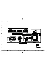
RF+
IFC
SW5V
GND
TU.RCH
RR+
VDD
CD.RESET
LR+
SW3
LCD.CE
TU.LCH
CD8V
SDA
DETACH
R5V
LF+
DETACH
CD.RCH
RF-
RR-
LR-
LF-
9V
SCL
ILL_10V
EO
FM.OSC
CD.LCH
9V
LRO
RRO
CD8V
MUTE
MCLK
MDATA
MCLK
MLD
CD.SENSE
SW2
SQCK
SUBQ
STATUS
CD.RESET
REST
SW1
SW2
LM1
LM0
SW4
R5V
TLOCK
MDATA
FLOCK
MLD
BLKCK
REMOCON
LCD.SCK
LCD.SO
KEY0
KEY1
KEY2
SDA
SCL
AGC
SW1
SW3
REST
SQCK
ILL_10V
LCD.CE
LCD.SCK
CD.SENSE
LM0
STATUS
LM1
EO
S.METER
IFC
SUBQ
SW4
LCD.SO
SW5V
TU.RCH
FM/AM
LF+
SD/ST
CD.RCH
KEY2
CD.LCH
MONO
LRO
LR+
LF-
ILL_10V
LR-
RF-
MUTE
SD/ST
RR+
RRO
RR-
TU.LCH
REMOCON
KEY1
9V
S.METER
BLKCK
MONO
TLOCK
FLOCK
FM/AM
AGC
KEY0
FM.OSC
RF+