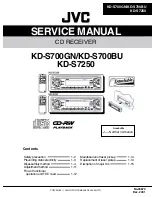


SERVICE MANUAL
CD RECEIVER
No.49670
Dec. 2001
COPYRIGHT 2001 VICTOR COMPANY OF JAPAN, LTD.
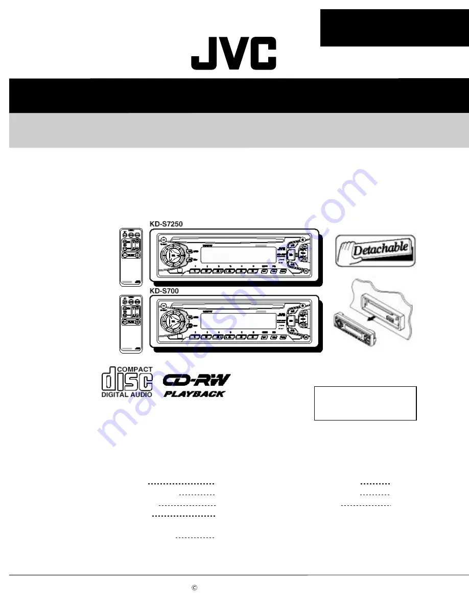
KD-S700GN/KD-S700BU
KD-S7250
KD-S700GN/KD-S700BU
KD-S7250
Area Suffix
J ----Northern America
Contents
Safety precaution
Preventing static electricity
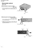
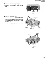
Disassembly method
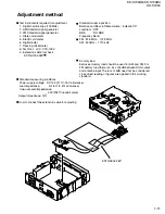
Adjustment method
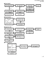
Flow of functional
operation unit TOC read
1-2
1-3
1-4
1-11
1-12
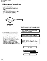
Maintenance of laser pickup
Replacement of laser pickup
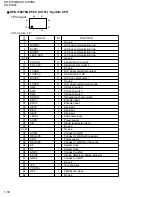
Discription of major ICs
1-14
1-14
1-15