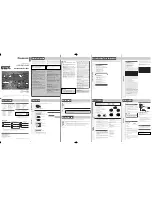

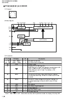


A
B
C
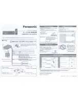
1
2
3
4
5
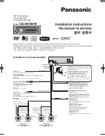
KD-S700GN/KD-S700BU
KD-S7250
2-6
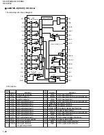
BZ841
C1
C2
C3
C5
C12
C14
C16
C17
C18
C21
C22
C31
C32
C33
C35
C41
C42
C81
C82
C83
C84
C161
C163
C164
C165
C166
C167
C171
C174
C175
C176
C177
C178
C179
C180
C181
C182
C185
C186
C191
C192
C195
C196
C201
C202
C205
C211
C212
C215
C216
C242
C243
C244
C245
C300
C308
C309
C317
C318
C319
C320
C321
C331
C333
C341
C351
C361
C362
C363
C364
C501
C502
C503
C504
C505
C507
C508
C509
C510
C511
C512
C521
C522
C523
C524
C525
C526
C527
C528
C530
C531
C533
C534
C535
C536
C537
C538
C539
C540
C541
C544
C545
C546
C547
C548
C549
C550
C551
C552
C553
C554
C561
C562
C563
C572
C582
C587
C591
C592
C593
C594
C597
C701
C702
C703
C705
C706
C707
C708
C709
C710
C801
C802
C803
C841
C891
C901
C902
C903
C904
C905
C906
C907
C908
C909
C910
C912
C913
C915
C975
C976
C977
CJ1
CJ321
CJ322
CN901
D1
D2
D21
D22
D31
D101
D242
D243
D244
D245
D301
D331
D341
D561
D901
D903
D976
D977
IC302
IC901
L1
L521
L522
L523
L524
L701
L702
L901
LM0
LM1
Q1
Q2
Q21
Q22
Q23
Q31
Q32
Q41
Q42
Q241
Q301
Q501
Q521
Q522
Q561
Q841
Q891
Q963
Q964
Q976
Q977
R1
R2
R3
R5
R8
R9
R10
R21
R22
R23
R24
R25
R26
R27
R32
R33
R34
R42
R43
R81
R82
R83
R84
R162
R163
R172
R173
R175
R176
R181
R182
R191
R192
R201
R211
R241
R242
R243
R244
R245
R246
R247
R248
R249
R321
R322
R332
R342
R351
R352
R501
R502
R503
R504
R505
R506
R507
R508
R509
R510
R511
R512
R513
R514
R515
R516
R517
R521
R522
R523
R524
R525
R526
R527
R528
R529
R530
R531
R532
R534
R535
R536
R537
R538
R539
R561
R562
R563
R564
R565
R566
R572
R573
R575
R582
R583
R585
R591
R592
R593
R594
R701
R702
R703
R706
R707
R708
R709
R710
R711
R712
R713
R714
R715
R716
R717
R719
R721
R723
R724
R725
R726
R728
R729
R731
R732
R733
R734
R735
R739
R744
R745
R746
R747
R748
R749
R750
R801
R803
R804
R805
R806
R807
R808
R809
R810
R811
R812
R813
R814
R815
R841
R842
R891
R892
R893
R901
R905
R906
R967
R968
R976
RESET
TP1
TP2
TU1
VDD
VPP
VSS
X1
X521
X701
C85
D706
C711
B301
D707
D705
D701
D702
D708
D703
D709
D704
C24
D971
D972
Q971
R971
R972
R4
C555
C601
C602
C603
C611
C681
C682
CJ601
D644
IC602
R606
R607
R611
R612
R613
R614
R615
R631
R636
R637
R640
R641
R642
R643
R646
R647
R651
R652
R653
R654
R656
R657
R658
R661
R662
R681
D645
R659
R649
R648
C612
D642
D643
D641
R660
D646
15
1
1
T1C
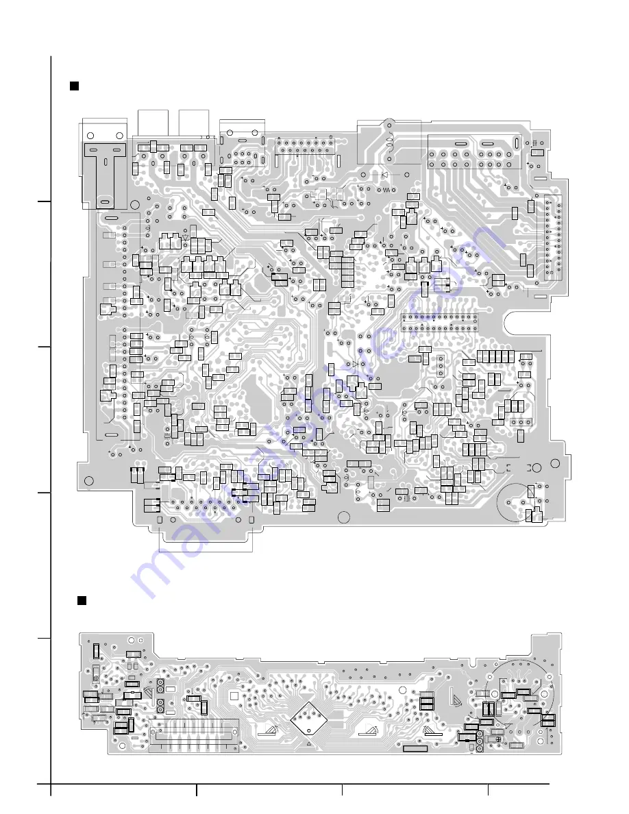
Main board(Reverse side)
Front board(Reverse side)