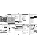
SERVICE MANUAL
CD RECEIVER
No.49676
Feb. 2002
COPYRIGHT 2002 VICTOR COMPANY OF JAPAN, LTD.
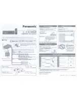
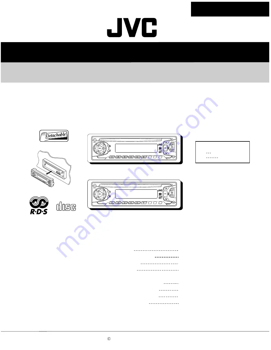
KD-S733R/KD-S731R
KD-S733R/KD-S731R
Area Suffix
E
EX
Continental Europe
Central Europe
COMPACT
DIGITAL AUDIO
45Wx4
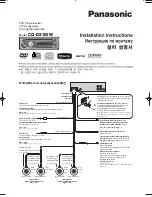
KD-S731R
7
8
9
10
11
12
RDS
MO
RND
DISP
TP
PTY
SCM
KD-S731R
45Wx4
KD-S733R
7
8
9
10
11
12
RDS
MO
RND
DISP
TP
PTY
SCM
KD-S733R
Contents
Safety precaution
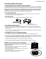
Preventing static electricity
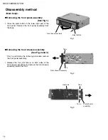
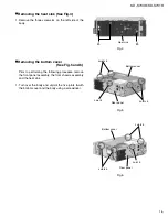
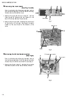
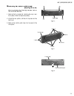
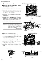
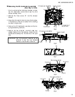
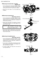
Disassembly method
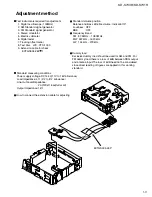
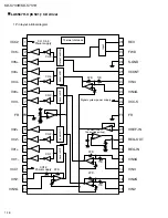
Adjustment method
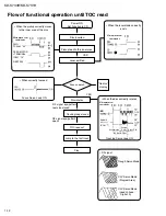
Flow of functional operation
untill TOC read
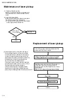
Maintanance of laser pickup
Replacement of laser pickup
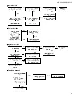
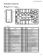
Description of major ICs
1- 2
1- 3
1- 4
1-11
1-12
1-14
1-14
1-15~29