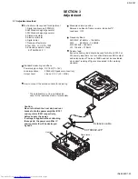
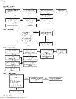
KD-S747
(No.49822)1-29
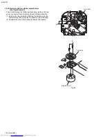
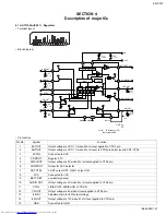
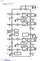
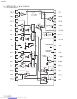
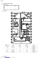
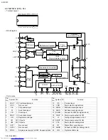
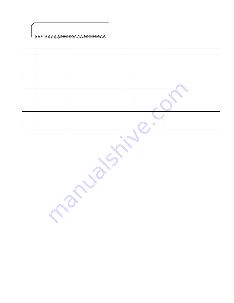
• Pin layout
• Pin function
TA
B
GND
FR-
STDBY
FR+
VP1
RR-
GND
RR+
RIPPLE
INRF
INRR
SGND
FLIN
RLIN
DNTIME
RL+
GND
RL-
VP3
FL+
MUTE
FL-
GND
NC
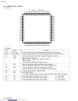
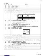
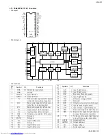
Pin No.
Symbol
Function
Pin No.
Symbol
Function
1
TAB
Header of IC
14
FLIN
Front Lch input
2
GND
Power GND
15
RLIN
Rear Lch input
3
FR-
Outpur(-) for front Rch
16
ONTIME
Power on time control
4
STDBY
Stand by input
17
RL+
Output (+) for rear Lch
5
FR+
Output (+) for front Rch
18
GND
Power GND
6
VP1
Power input
19
RL-
Output (-) for rear Lch
7
RR-
Output (-) for rear Rch
20
VP3
Power input
8
GND
Power GND
21
FL+
Output (+) for front
9
RR+
Output (+) for rear Rch
22
MUTE
Muting control input
10
RIPPLE
Ripple filter
23
FL-
Output (-) for front
11
RRIN
Rear Rch input
24
GND
Power GND
12
FRIN
Front Rch input
25
NC
Non connection
13
SGND
Signal GND