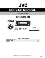


SERVICE MANUAL
COPYRIGHT © 2003 VICTOR COMPANY OF JAPAN, LTD.
No.49820
2003/04
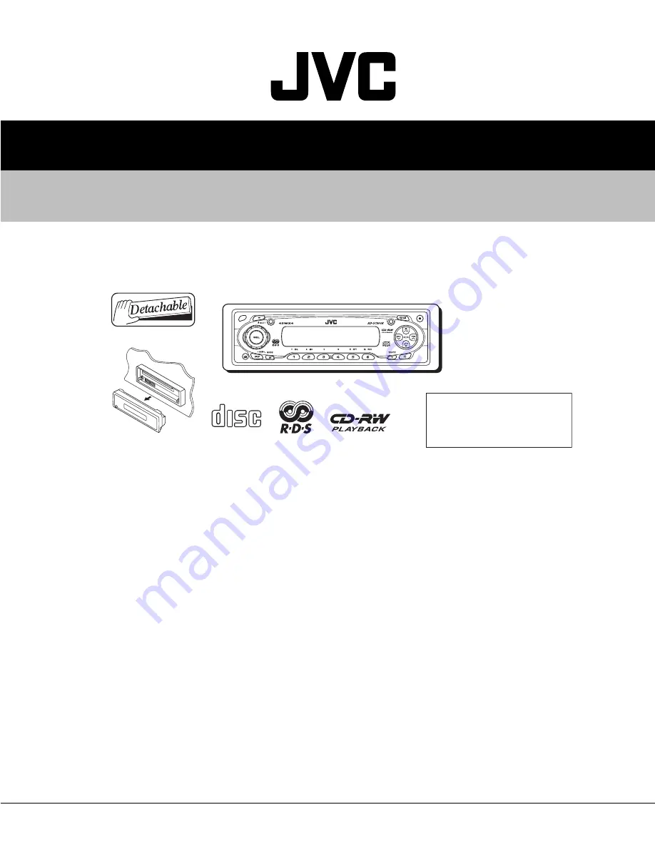
KD-SC800R
CD RECEIVER
49820
2003
04
KD-SC800R
TABLE OF CONTENTS
1
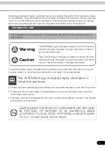
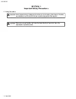
Important Safety Precautions . . . . . . . . . . . . . . . . . . . . . . . . . . . . . . . . . . . . . . . . . . . . . . . . . . . . . . . . . . . 1-2
2
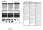
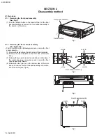
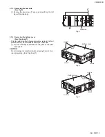
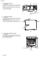
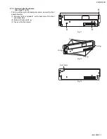
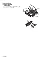
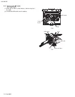
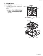
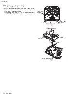
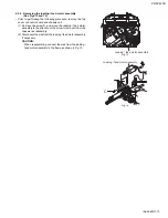
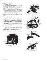
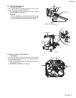
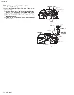
Disassembly method . . . . . . . . . . . . . . . . . . . . . . . . . . . . . . . . . . . . . . . . . . . . . . . . . . . . . . . . . . . . . . . . . . 1-4
3
Adjustment. . . . . . . . . . . . . . . . . . . . . . . . . . . . . . . . . . . . . . . . . . . . . . . . . . . . . . . . . . . . . . . . . . . . . . . . . . 1-24
4
Description of major ICs. . . . . . . . . . . . . . . . . . . . . . . . . . . . . . . . . . . . . . . . . . . . . . . . . . . . . . . . . . . . . . . 1-28
COMPACT
DIGITAL AUDIO
Area Suffix
E ------------ Continental Europe
EX --------------- Central Europe
Summary of Contents for KD-SC800R
Page 67: ...KD SC800R 3 11 MEMO ...