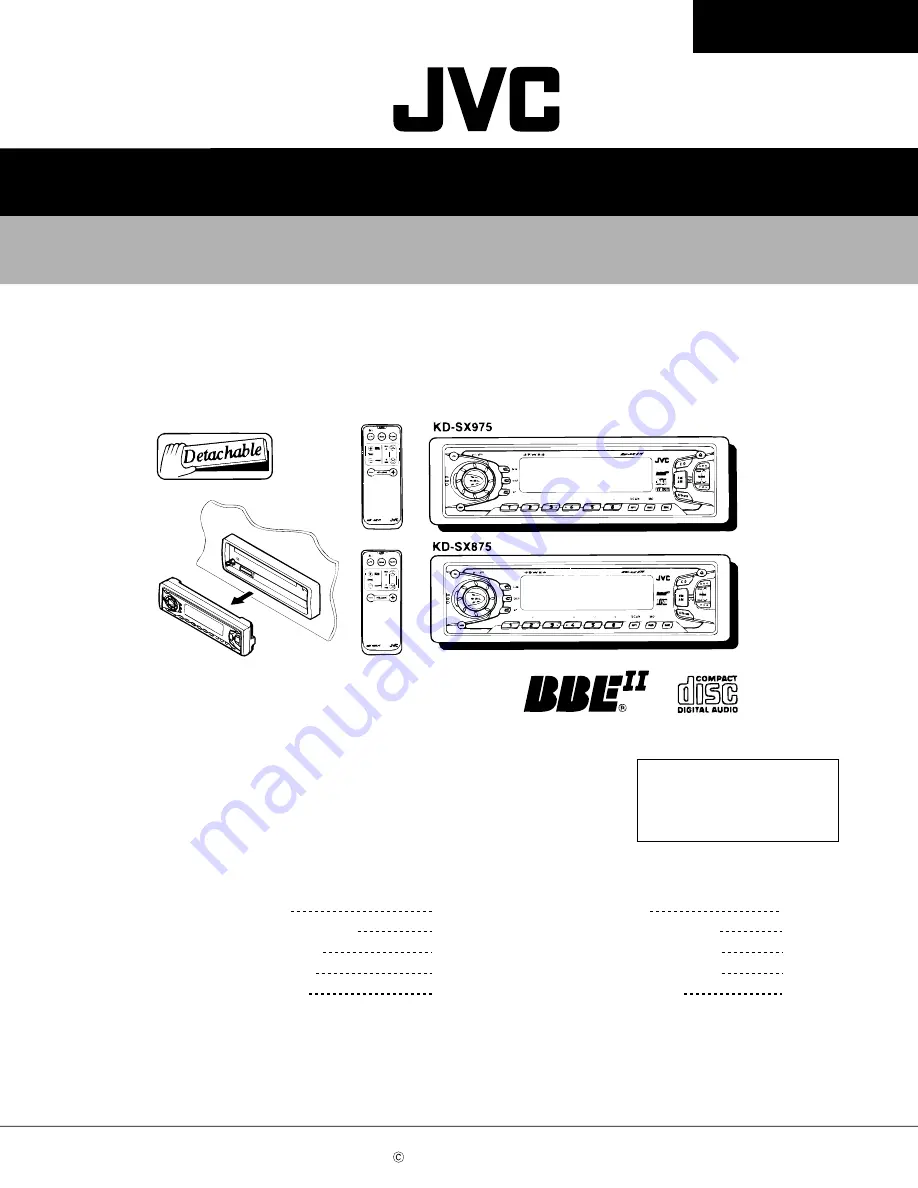
SERVICE MANUAL
CD RECEIVER
No.49620
Feb. 2001
COPYRIGHT 2001 VICTOR COMPANY OF JAPAN, LTD.
KD-SX975 / KD-SX875
KD-SX975 / KD-SX875
Area Suffix
U ---- Other Areas
Contents
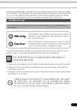
Safety precaution
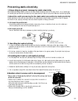
Preventing static electricity
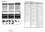
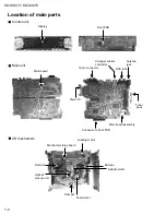
Location of main parts
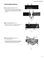
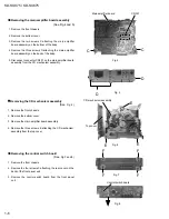
Disassembly method
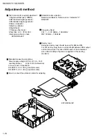
Adjustment method
1-2
1-3
1-4
1-5
1-10
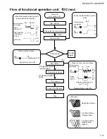
Flow of functional
operation unit TOC read
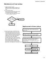
Maintenance of laser pickup
Replacement of laser pickup
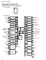
Discription of major ICs
1-11
1-13
1-13
1-14
Summary of Contents for KD-SX875
Page 33: ... M E M O KD SX975 KD SX875 2 2 ...