background image

KS-F171

(No.49774)1-19

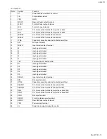
• Pin functions

Pin No

Symbol

Function

1

DI

Serial data input terminal for control

2

CE

Chip enable terminal

3

VSS

GND

4

LROUT

Rear Lch fader output terminal

5

LFOUT

Front Lch fader output terminal

6

LFIN

Front Lch input terminal

7

LOUT

C & R connection terminal for super bass band

8

LSB

C & R connection terminal for super bass band

9

LBASS2

C & R connection terminal for bass band

10

LBASS1

C & R connection terminal for bass band

11

LTRE

Capacitor connection terminal for treble band filter

12

LIN

Lch input terminal

13

LSELO

Input selector output terminal

14

L5

input signal terminal

15

L4

input signal terminal

16

L3

input signal terminal

17

L2

input signal terminal

18

L1

input signal terminal

19

Vref

Power supply for analog GND

20

R1

input signal terminal

21

R2

input signal terminal

22

R3

input signal terminal

23

R4

input signal terminal

24

R5

input signal terminal

25

RSELO

Input selector output terminal

26

RIN

Rch input terminal

27

RTRE

Capacitor connection terminal for treble band filter

28

RBASS1

C & R connection terminal for bass band filter

29

RBASS2

C & R connection terminal for bass band filter

30

RSB

C & R connection terminal for super bass band filter

31

ROUT

C & R connection terminal for super bass band filter

32

RFIN

Rch input terminal

33

RFOUT

Front Rch fader output terminal

34

RROUT

Rear Rch fader output terminal

35

VDD

Power supply terminal

36

CL

Serial clock output terminal for control

Summary of Contents for KS-F171

Page 1: ...APAN LTD No 49774 2003 01 KS F171 CASSETTE RECEIVER 49774 2003 01 KS F171 TABLE OF CONTENTS 1 Important Safety Precautions 1 2 2 Disassembly method 1 3 3 Adjustment method 1 12 4 Description of major ICs 1 16 Area Suffix U Other Areas S BASS SEL DISP ...

Page 2: ... SECTION 1 Important Safety Precautions 1 1 Safety Precautions Burrs formed during molding may be left over on some parts of the chassis Therefore pay attention to such burrs in the case of preforming repair of this system ...

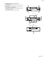
Page 3: ...oints b on the right side and the joint c on the back of the body then remove the bottom cover from the body CAUTION When releasing the joint c using a screwdriver do not damage the board Fig 2 2 1 3 Removing the front chassis See Fig 3 Prior to performing the following procedure remove the front panel assembly and bottom cover 1 Remove the screw A on each side of the body 2 Release the two joints...

Page 4: ... the front panel assembly and bottom cover 1 Remove the two screws D one screw E and three screws F attaching the rear panel on the back of the body Fig 5 2 1 6 Removing the main board See Fig 6 Prior to performing the following procedure remove the front panel assembly bottom cover front chassis heat sink and rear panel 1 Remove the two screws G attaching the main board on the top chassis 2 Disco...

Page 5: ...oard See Fig 8 Prior to performing the following procedure remove the front panel assembly bottom cover front chassis heat sink rear panel main board and cassette mechanism assembly 1 Disconnect the wire from CJ901 on the head amplifier board 2 Remove the one screw J attaching the head amplifier board 3 Move the head amplifier board in the direction of the arrow to release the two joints f the hea...

Page 6: ...rew K attaching the relay board 3 Move the relay board in the direction of the arrow to release the joint g the relay board can be removed Fig 9 2 1 10 Removing the mecha bracket See Fig 10 Prior to performing the following procedure remove the front panel assembly bottom cover front chassis heat sink rear panel main board cassette mechanism assembly head am plifier board and relay board 1 Remove ...

Page 7: ...e the front panel assembly 1 Remove the four screws M attaching the rear cover on the back of the front panel assembly 2 Release the eleven joints h the front panel and the rear cover become separate 3 Remove the switch board from the rear cover Fig 11 Fig 12 Fig 13 M M M M Joint h Joint h Joint h Joint h Switch LCD Key board ...

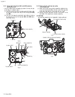
Page 8: ...remove the direc tion switch board and the FF REW lever assembly 1 Remove the screw D attaching the playback head 2 Remove the C washer and pull out the FF roller 3 Remove the S support plate the A arm spring a and b the playback head ATTENTION The A arm spring a differs from the A arm spring b 2 2 5 Removing the pinch roller R and F assembly See Fig 2 Prior to performing the following procedure r...

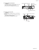
Page 9: ...embly See Fig 4 Prior to performing the following procedure remove the FF REW lever assembly and the cassette hanger cassette hold er 1 Remove the C washer and pull out reel disc assembly ATTENTION Replace with a new C washer when reattaching Fig 4 2 2 8 Removing the motor assembly See Fig 5 1 Unsolder the two wires j on the motor assembly 2 Turn over the cassette mechanism assembly and remove the...

Page 10: ...ng the reel base assembly See Fig 5 and 6 1 Raise the part k of the reel base assembly slightly and re move the selector link B on the front side of the cassette mechanism assembly by turning it as shown in Fig 6 2 Remove the three screws E and the one screw F on the underside of the cassette mechanism assembly ATTENTION The reel base assembly is not repairable Handle with care Fig 6 Fig 7 Reel di...

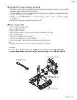
Page 11: ... board Fig 8 2 2 12 Removing the power switch See Fig 9 Prior to performing the following procedure remove the motor assembly 1 Unsolder the two wires m on the power switch on the side of the cassette mechanism assembly 2 Remove the screw I attaching the power switch Fig 9 Cassette mechanism assembly Soldering l H Mute switch board Rower switch Motor assembly Soldering m I Power switch Cassette me...

Page 12: ...or CTG N Mechanism adjustment VT724 for DOLBY level measurement VT739 For playback frequency measurement VT712 For wow flutter tape speed measurement VT703 For head azimuth measurement Balance and Bass Treble volume Fader Center Indication 0 Loudness Dolby NR Sound Cruise Off Volume position is about 2V at speaker output with following conditions Playback the test tape VT721 Power supply voltage D...

Page 13: ...tach a heat sink on the power amplifier IC of a main board when supplying the power If voltage is applied without attaching the heat sink the power amplifier IC will be destroyed by heat 1 For 1995 and 1996 we re advancing efforts to make our extension cords common for all car audio products Please use this type of extension cord as follows 2 As a U shape type top cover is employed this type of ex...

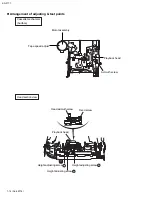
Page 14: ...ead azimuth screw Cassette mechanism Surface Tape speed adjust Motor assembly Fixed screw Height adjusting screw c Height adjusting screw b Height adjusting screw a Playback head Playback head Azimuth screw Arrangement of adjusting test points ...

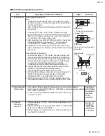
Page 15: ...1 Load the test tape VT724 1kHz and play it back in the reverse play mode set the Rch output level to maximum 2 Load the test tape VT703 10kHz and play it back in the forward play mode Adjust the Rch and Lch output levels to maximum with azimuth adjustment screw b In this case the phase difference should be within 45 3 Engage the reverse mode and adjust the output level to maximum with azimuth adj...

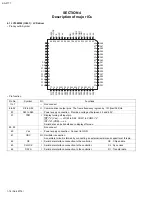
Page 16: ...I O Oscillator connection An oscillator circuit is formed by connecting an external resistor and capacitor at this pin 62 CE I Serial data interface connection to the controller CE Chip enable 63 CLOCK I Serial data interface connection to the controller CL Sync clock 64 DATA I Serial data interface connection to the controller DI Transfer data 1 2 3 4 5 6 7 8 9 10 11 12 13 14 15 16 S8 S9 S10 S11 ...

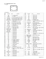
Page 17: ...onaural and stereo change over output 36 R T Non connect 37 NC Non connect 38 POWER CNT O Power control output 39 NC Non connect 40 NC Non connect 41 IF CONT Non connect 42 NC Non connect 43 NC Non connect 44 NC Non connect 45 NC Non connect 46 NC Non connect 47 NC Non connect 48 TAPE IN I H RADIO L TAPE 49 F R SENCE I FORWARD REVERSE switch de tector 50 TAPE MUTE I DIR FF REW MUTE 51 SD ST I Stat...

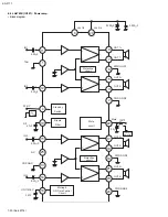
Page 18: ...75421M X IC931 E volume Pin layout Block diagram 36 19 1 18 34 33 32 31 30 29 28 27 26 25 24 23 22 21 20 19 18 17 16 15 14 13 12 11 10 9 8 7 6 5 4 3 2 1 36 35 CCB INTERFACE CONTROL CIRCUIT LOGIC CIRCUIT CONTROL CIRCUIT LVref RVref ...

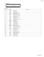
Page 19: ... signal terminal 16 L3 input signal terminal 17 L2 input signal terminal 18 L1 input signal terminal 19 Vref Power supply for analog GND 20 R1 input signal terminal 21 R2 input signal terminal 22 R3 input signal terminal 23 R4 input signal terminal 24 R5 input signal terminal 25 RSELO Input selector output terminal 26 RIN Rch input terminal 27 RTRE Capacitor connection terminal for treble band fil...

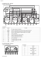
Page 20: ... Vcc 1 2 Vcc 3 4 OUT 1 OUT 1 PWR GND1 OUT 2 OUT 2 PWR GND2 R F IN 3 IN 4 PRE GND ON TIME C Muting ON Time Control Circuit Protective circuit Protective circuit Mute circuit Ripple Filter Stand by Switch N C 0 22 F 2200 F 0 022 F 0 22 F TAB 5V ST ON 47 F 0 22 F 0 22 F 22 F Mute 10K 3 3 F OUT 3 OUT 3 Low Level Mute ON PWR GND3 OUT 4 OUT 4 PWR GND4 ...

Page 21: ...t 5 FR Output for front Rch 6 VP1 Power input 7 RR Output for rear Rch 8 GND Power GND 9 RR Output for rear Rch 10 RIPPLE Ripple filter 11 RRIN Rear Rch input 12 FRIN Front Rch input 14 FLIN Front Lch input 15 RLIN Rear Lch input 16 ONTIME Power on time control 17 RL Output for rear Lch 18 GND Power GND 19 RL Output for rear Lch 20 VP3 Power input 21 FL Output for front 22 MUTE Muting control inpu...

Page 22: ...power supply 6 AMP Power supply supply to remote amplifier 7 VCC Back up connects with ACC with it 8 ANT Power supply supply to auto antenna 9 COM 8 7V power supply 10 AM The power supply of 8 7V to AM 11 FM The power supply of 8 7V to FM 12 GND Ground Pre Drive Thermal Protection Reference Voltage Pre Drive AMP Out ASO Peak Current Protection AMP Out Pre Drive Pre Drive Pre Drive 1 2 3 4 5 6 7 8 ...

Page 23: ...KS F171 No 49774 1 23 ...

Page 24: ... No 49774 AV MULTIMEDIA COMPANY 10 1 1chome Ohwatari machi Maebashi city 371 8543 Japan VICTOR COMPANY OF JAPAN LIMITED 200301WPC Printed in Japan KS F171 ...

Reviews: