background image

SERVICE MANUAL

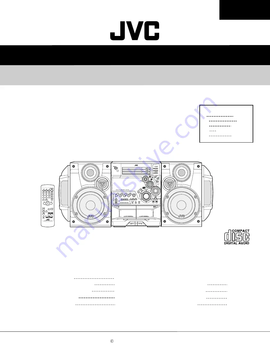
COMPACT COMPONENT SYSTEM

  No.20986

Jun. 2001

COPYRIGHT      2001 VICTOR COMPANY OF JAPAN, LTD.

MX-G70

MX-G70

Area Suffix            

A
UP
US
UW
UY

Australia

Korea 

Singapore

Brazil,Mexico,Peru

Argentina

This service manual is printed on 100% recycled paper.

Safety precautions
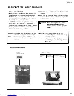
Important for laser products
Preventing static electricity
Disassembly method
Adjustment method

1-2
1-3
1-4
1-5
1-25

Flow of functional operation
                       until TOC read
Maintenance of laser pickup
Replacement of laser pickup
Description of major ICs  

1-29
1-30
1-30
1-31~49

Contents

PLAY & EXCHANGE

STANDBY/ON

CD-R

/RW  PLAYBACK

STANDBY

MX-G70

CA-MXG70

SP-MXG70

SP-MXG70

(No MIC jack and MIC LEVEL volume for A,UP,UY ver.)

Summary of Contents for MX-G70

Page 1: ...cycled paper Safety precautions Important for laser products Preventing static electricity Disassembly method Adjustment method 1 2 1 3 1 4 1 5 1 25 Flow of functional operation until TOC read Maintenance of laser pickup Replacement of laser pickup Description of major ICs 1 29 1 30 1 30 1 31 49 Contents PLAY EXCHANGE STANDBY ON CD R RW PLAYBACK STANDBY MX G70 CA MXG70 SP MXG70 SP MXG70 No MIC jac...

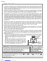
Page 2: ...inet screw heads headphone jack control shafts etc to be sure the product is safe to operate without danger of electrical shock Do not use a line isolation transformer during this check Plug the AC line cord directly into the AC outlet Using a Leakage Current Tester measure the leakage current from each exposed metal parts of the cabinet particularly any exposed metal part having a return path to ...

Page 3: ...aserstrålning är denna del är öppnad och spårren är urkopplad Betrakta ej strålen VARO Avattaessa ja suojalukitus ohitettaessa olet alttiina näkymättömälle lasersäteilylle Älä katso säteeseen ADVARSEL Usynlig laserstråling ved åbning når sikkerhedsafbrydere er ude af funktion Undgå udsættelse for stråling ADVARSEL Usynlig laserstråling ved åpning når sikkerhetsbryteren er avslott unngå utsettelse ...

Page 4: ...rce can easily destroy the laser diode 4 Handling the traverse unit optical pickup 1 Do not subject the traverse unit optical pickup to strong shocks as it is a sensitive complex unit 2 Cut off the shorted part of the flexible cable using nippers etc after replacing the optical pickup For specific details refer to the replacement procedure in the text Remove the anti static pin when replacing the ...

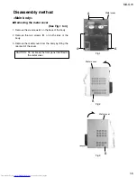
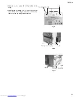
Page 5: ...es of the body Remove the metal cover from the body by lifting the rear part of the cover 1 2 3 Disassembly method Main body Removing the metal cover See Fig 1 to 3 Do not break the front panel tab fitted to the metal cover CAUTION Fig 1 Fig 2 Fig 3 A A A Metal cover Metal cover B Metal cover B ...

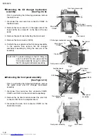
Page 6: ...ger mechanism assembly Disconnect the card wires from connector CN870 CN871 and CN315 on the main board respectively Remove the tie band and disconnect the wire from connector CN703 on the amplifier board Disconnect the wire from connector CN220 on the transformer board 1 2 3 Removing the front panel assembly See Fig 6 to 10 To prevent damage to the CD fitting be sure to pull both the rear panel a...

Page 7: ...body Release the two joints a on the lower right and left sides of the body using a screwdriver and remove the front panel assembly toward the front 4 5 Fig 8 Fig 9 Fig 10 E Bottom Front panel assembly Joint a Joint a Front panel assembly Front panel assembly ...

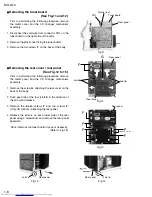
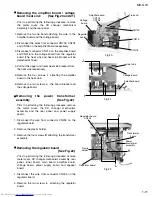
Page 8: ... Remove the screw G attaching the rear cover on the back of the body Push each tab of the four joints b in the direction of the arrow and release Remove the twelve screws F and two screws F Only US UW ver attaching the rear panel Release the joints c on each lower side of the rear panel using a screwdriver and remove the rear panel backward 1 2 3 4 Removing the rear cover rear panel See Fig 12 to ...

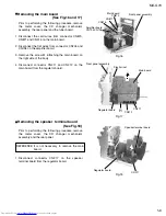
Page 9: ... on the main board from the regulator board 1 2 3 4 Removing the main board See Fig 16 and 17 Prior to performing the following procedure remove the metal cover the CD changer mechanism assembly and the rear panel Disconnect connector CN217 on the speaker terminal board from the regulator board 1 Removing the speaker terminal board See Fig 18 It is not necessary to remove the main board REFERENCE ...

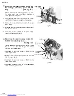
Page 10: ...oltage selector only US UW ver See Fig 19 1 Removing the power supply board On the ECO Circuit Only A ver See Fig 19 2 Prior to performing the following procedure remove the metal cover the CD changer mechanism assembly and the rear panel Disconnect the wire from connector CN250 on the power supply board Move the power cord stopper upward and pull out it from the base chassis Disconnect the wire f...

Page 11: ...the metal cover the CD changer mechanism assembly and the rear panel Remove the two tie band attaching the wire to the amplifier board and the voltage board Disconnect the wires from connector CN703 CN704 and CN706 on the amplifier board respectively Disconnect connector CN215 on the amplifier board and CN216 on the voltage board from the regulator board The heat sink and heat sink bracket will be...

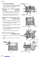
Page 12: ...s O attaching the display system control board If necessary disconnect the wire from connector CN911 on the front side of the display system control board and unsolder FW915 If necessary remove the CD play board Fig 29 1 2 3 4 Removing the display system control board See Fig 24 to 26 Remove the three screws P attaching the CD eject board If necessary unsolder FW915 on the CD eject board 1 2 Remov...

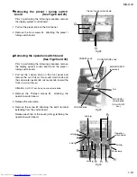
Page 13: ...b and the sub woofer level knob mic level knob toward the front Only US UW ver Attention A UP UY ver have no mic volume knob Remove the Thirteen screws R attaching the operation switch board Release the wire clamp Remove the screw R attaching the earth terminal extending from the switch board Release each tab of the seven joints g retaining the operation switch board 1 2 3 4 Removing the operation...

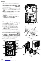
Page 14: ...Fig 4 By removing the pawl at the section d fixing the return spring dismount the return spring See Fig 4 Remove the three lock levers See Fig 4 10 11 Fig 1 Fig 2 Fig 3 Fig 4 1 Remove the metal cover 2 Remove the CD changer mechanism assembly 3 From bottom side the CD changer mechanism assembly remove the four screws A retaining the CD servo control board 4 Absorb the four soldered positions a of ...

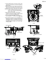
Page 15: ...15 Manually turn the motor pulley in the clockwise direction until the lifter unit stopper is lowered from the section e of CD tray assembly See Fig 8 Pull out all of the three stages of CD tray assembly in the arrow direction f until these stages stop See Fig 6 At the position where the CD tray assembly has stopped pull out the CD tray assembly while pressing the two pawls g and g on the back sid...

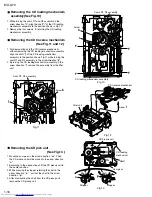
Page 16: ...tion k By raising the CD loading mechanism assembly in the arrow direction l remove the assembly from the lifter unit Fig 10 Fig 12 Fig 11 Fig 13 Removing the CD pick unit See Fig 13 1 2 3 4 Move the cam gear in the arrow direction m Then the CD pickup unit will be moved in the arrow direction n According to the above step shift the CD pickup unit to the center position While pressing the stopper ...

Page 17: ...m gear q align the Paul r position of the drive unit to the notch position Fig 16 on the cam gear q Pull out the drive unit and cylinder gear See Fig 17 While turning the cam gear q align the Paul s position of the select lever to the notch position Fig 18 on the cam gear q Remove the four screws H retaining the cam unit cam gear q and cams R1 R2 assembly See Fig 18 Cam gear q Drive unit r G H J H...

Page 18: ... in the arrow direction remove the gear bracket See Fig 18 From the notch u section on the chassis assembly fixing the edge of gear bracket remove and take out the gear bracket See Fig 19 Remove the belts respectively from the right and left actuator motor pulleys and pulley gears See Fig 18 After turning over the chassis assembly remove the actuator motor while spreading the four pawls v fixing t...

Page 19: ...m gear q See Fig 22 1 2 3 4 Remove the slit washer fixing the cams R1 and R2 assembly By removing the two pawls w fixing the cam R1 separate R2 from R1 Remove the slit washer fixing the cam gear q Pull out the cam gear q from the C G base assembly Removing the C G base assembly See Fig 22 and 23 Remove the three screws J retaining the C G base assembly Fig 23 Slit washer Pawl Cam R2 Slit washer Ca...

Page 20: ...th screw retaining the playback head 7 Take out the playback head from the front of the head mount 8 The recording and eraser heads should also be removed similarly according to Steps 1 7 above Reassembling the playback recording and eraser heads See Fig 3 1 Reassemble the playback head from the front of the head mount to the position as shown in Fig 3 2 Fix the reversing azimuth screw 3 Set the s...

Page 21: ...ssembly See Fig 5 to 7 1 Remove the six screws B retaining capstan motor assembly See Fig 5 2 While raising the capstan motor remove the capstan belts A and B respectively from the motor pulley See Fig 6 Caution 1 Be sure to handle the capstan belts so carefully that these belts will not be stained by grease and other foreign matter Moreover these belts should be hand while referring to the capsta...

Page 22: ...fixing the capstan shafts R and L and pull out the flywheels R and L respectively from behind the cassette mechanism Removing the reel pulse board and solenoid See Fig 11 1 Remove the five pawls c d e f g retaining the reel pulse P C Board 2 From the surface of the reel pulse P C Board parts remove the two pawls h and i retaining the solenoid Capstan motor Joint bracket Flywheel R Flywheel L Flywh...

Page 23: ...the following procedure remove the side cover Remove the four screws C respectively Remove the front cover toward the front and disconnect the yellow and black wires from the tweeter speaker terminals Removing the front cover See Fig 3 to 4 Attention which adheres to speaker box The speaker box of this model is a unit supply Therefore we do not supply it as individual parts though the method of di...

Page 24: ... disconnect the wire yellow and black blue and black from the two speaker terminals 1 2 Removing the woofer speaker See Fig 5 Prior to performing the following procedure remove the side cover and the front cover Remove the two screws F attaching the tweeter speaker on the back of the front cover 1 Removing the tweeter speaker See Fig 6 Fig 5 Fig 6 Woofer speaker F D Tweeter speaker Front cover D ...

Page 25: ... 30 FM modulation frequency 400Hz Frequency displacement 22 5kHz Frequency Range AM 531kHz 1710kHz UP US UW UY model 522kHz 1629kHz A model FM 87 5MHz 108MHz Standard measurement positions of volume and switch Power Standby Light STANDBY Indicator Sub woofer VOL Minimum Sound mode OFF Main VOL 0 Minimum Traverse mecha set position Disc 1 Mic MIX VOL MAX Only US UW ver ECHO OFF Precautions for meas...

Page 26: ...tion Back side Cassette Mechanism Unit Section Head azimuth adjusting screw Forward side Head azimuth adjusting screw Reverse side Head azimuth adjusting screw Forward side Head azimuth adjusting screw Reverse side Playback head Playback recording and eraser heads or playback head Tape speed ADJ Bias ADJ L Bias ADJ R ...

Page 27: ...corder section Items Measurement conditions Measurement method Standard values Adjusting positions After setting to the double speed motor confirm that the frequency counter reading becomes 4 800 400 300Hz when the test tape VTT712 3kHz has been play back with the playback mechanism When the test tape VTT712 3kHz has been played back with the playback mechanism or recording and playback mechanism ...

Page 28: ...inal Both recording and headphone terminals Reference frequency 1kHz and 10kHz REF 20dB Test tape TYP AC 225 Measurement input terminal OSC IN AC 225 4 20 A Output deviation between 1kHz and 10kH 1dB 2dB LcH VR101 RcH VR201 LcH VR101 RcH VR201 Electrical performance Items Measurement conditions Measurement method Standard values Adjusting positions 1 While changing over to and from BIAS 1 and 2 co...

Page 29: ...Automatic measurement of TE amplitude and automatic tuning of TE balance 500mv div 2ms div Fig 1 Approx 3sec pin 25 of IC601 TE Approx 1 8V VREF Tracking error waveform at TOC reading Power ON Play Key Confirm that the Focus error S cuve signal at the pin28 of IC651 is approx 2Vp p Confirm that the signal from pin24 IC651 is 0V as a accelerated pulse during approx 400ms Confirm the waveform of the...

Page 30: ... of the laser diode has expired the following symptoms will appear 1 The level of RF output EFM output ampli tude of eye pattern will below Is the level of RFOUT under 1 25V 0 22Vp p Replace it NO YES O K 3 Semi fixed resistor on the APC PC board The semi fixed resistor on the APC printed circuit board which is attached to the pickup is used to adjust the laser power Since this adjustment should b...

Page 31: ...mplifier input R1 R2 I Playback amplifier input NF2 Playback amplifier negative feedback OUT2 Playback amplifier output EQ2 I Equalizer CTL2 I Pre Amplifier input switching time constant RIN2 I Recording amplifier input RNF2 I Recording amplifier negative feedback ROUT2 O Recording amplifier output O LC I ALC low cut LPF I ALC low pass filter GND I Vcc Power supply RF I Ripple filter EQCTL EQ cont...

Page 32: ...1 IN1 2 IN1 3 VEE 4 BA15218F XE IC652 BA15218N IC481 501 502 526 571 Dual op amp 1 Pin layout 2 Block diagram Q19 Q17 Q16 OTHER CH R9 R6 R8 R7 R5 R4 R3 R2 R1 D1 C1 Q18 Q13 Q11 Q8 Q5 Vcc VEE OUTPUT IN IN Q1 Q3 Q4 Q2 C2 Q9 Q6 Q7 Q10 Q12 Q14 Q15 Q114 ...

Page 33: ... Q7 Q8 Q s Qs 1 2 3 4 5 6 7 8 16 15 14 13 12 11 10 9 1 Pin layout 8 STAGE SHIFT REGISTER 8 BIT LATHES 3 STATE OUTPUTS 1 2 3 15 Q1 Q8 10 9 DATA CLOCK STROBE OUTPUT ENABLE PARALLEL OUTPUT Q s Qs SERIAL OUTPUT 2 Block diagram BU4094B IC303 Serial to parallel port extension 1 2 3 Pin No 1 2 3 Function Vcc Ground OUT KIA7019AP IC830 Voltage detector 1 Pin layout 2 Pin function ...

Page 34: ...ut Output Mode IN1 IN2 OUT1 OUT2 Brake 0 0 0 0 1 0 1 0 0 1 0 1 1 1 0 0 CLOCKWISE COUNTER CLOCKWISE Brake LB1641 IC851 IC852 DC motor driver 1 Pin layout 2 Pin function 1 2 3 4 5 6 7 8 1 A OUTPUT 2 A INPUT 3 A INPUT 4 V 5 B INPUT 6 B INPUT 7 B OUTPUT NJM4580L IC901 Mic Amplifier ...

Page 35: ...al Output selection control terminal Output selection control terminal Output selection control terminal Output selection control terminal Non connect Non connect Connected to GND upon normal use Multi plexor output terminal Connect to GND I O O O O O No Symbol I O Function 2 Pin Function 1 Block Diagrams BA3835S IC812 SPI B P F 1 2 3 4 5 6 7 8 9 18 17 16 15 14 13 12 11 10 BIAS VREF REFERENCE CURR...

Page 36: ...K TK LIN BIAS GND RIN LPF1 LPF2 LPF3 ROUT CONTA CONTB CONTC Power supply Microphone mixing input Channel L output Non connect Non connect Channel L input Signal bias Connect to GND Channel R input Connects to LPF time constant element Connects to LPF time constant element LPF outpout Channel R output Mode select input A Mode select input B Mode select input C I O I I I O O O O I I I Pin No Symbol ...

Page 37: ...T OUT ADINT IN VCC NC2 MUTE CR Connect GND Echo level control Non connect Analog part DC bias DA side integrator input DA side integrator output DA side LPF input DAside LPF output Mix AMP output for original tone echo tone Mix AMP input pin for original tone AD side LPF input AD side LPF output AD side integrator output AD side integrator input Power supply Non connect Mute control signal input C...

Page 38: ... AM OSC REG AM RF AFC AM AGC O I O I I I AM Local oscillation Signal output This is a terminal of AM Local oscillation circuit Register value between pin 26 and pin28 desides the frequency width of the input signal AM RF signal input This is an output terminal of voltage for FM AFC This is an AGC voltage input terminal for AM O O I O AM detection output FM detection output Mpx input terminal O O I...

Page 39: ...ts ON OFF BTL AMP 1 input pin BTL AMP 1 input pin For gain adjustment BTL AMP 1 input pin Non inverting side BTL AMP 1 input pin Inverting side BTL AMP 2 input pin Inverting side BTL AMP 2 input pin Non inverting side BTL AMP 2 input pin For gain adjustment BTL AMP 2 input pin External transistor collector PNP connection 5V power supply output External transistor PNP base connection Reset output R...

Page 40: ...ut output port Input output port Data input output Function IF counter signal input IF signal output Not use AM Local OSC signal output FM Local OSC signal input Power suplly VDD 4 5 5 5V When power ON Reset circuit move PLL charge pump output H Local OSC frequency Height than Reference frequency L Low Agreement Height impedance Input for active lowpassfilter of PLL Output for active lowpassfilter...

Page 41: ...TUNER data input SLC TUNER clock Not used Power supply 5V Oscillation terminal 8MHz Connect to GND Not used Connect to GND Connect to GND Key matrix input 1 4 SLC Key input 1 SLC Key input 2 Not used SPI Analog data input AD 5V VC3 Ready Micon reset Bass volume Bass volume Aux muting RDS Data Karaoke SPI A data SPI B data Remote control signal input SLC Photo A SLC Photo B Soundmode reverse RDS Cl...

Page 42: ...nt control signal output Tuner chip enable System mute Skip LED LED Control signal output CD1 LED Control signal output CD2 LED Control signal output CD3 Reverse skip Music scan input Tuner stereo indicator Backup mode detect Forward skip Rotary encoder VOL Rotary encoder VOL Soundmode foeward B for FL O O O O O O O I I I I I I I I Pin No Symbol I O Function Pin function 2 2 ...

Page 43: ... MDATA DSL PLL VCO AVDD2 SUB CODE BUFFER SSEL SQCK SUBQ AVDD2 CLVS CRC BLKCK CLDCK SBCK SUBC DEMPH RESY FLAG6 RESY EFM DEMODULATION SUBCODE DEMODULATION SYNC INTERPOLATION 16k SRAM CIRC ERROR CORRECTION DEINTERLEVE LRCKIN MSEL BCLK SSEL SRDATAIN PSEL IOSEL DIGITAL DEEMPHSIS 8TIMES OVER SAMPUNC DIGITAL FILTER 1BIT DAC LOGIC S PEM R PEM L DIGITAL AUDIO INTERFASE DIGITAL AUDIO INTERFASE INTER POLATIO...

Page 44: ... Tracking drive output Focus drive output Reference voltage input pin for D A output block TVD FOD FBA TBAL Focus Balance adjust signal output Tracking Balance adjust signal output Focus error signal input Analog input Tracking error signal input Analog input RF envelope signal input Analog input Vibration detect signal input H detect Off track signal input H off track Track cross signal input RF ...

Page 45: ...1 TR3 TR2 TR4 TR5 TR6 TR8 R8 C2 TR14 TR15 TR16 R14 R11 R13 R12 R10 R9 TR9 TR10 TR12 TR13 TR11 TR7 C1 D1 R6 R3 R4 R5 R7 13 11 14 15 9 8 12 5 6 7 10 2 R2 SUB STK402 030 IC602 Power amplifier 1 Pin layout 2 Block diagram 1 15 ...

Page 46: ...VOLUME TREBLE TREBLE MIDLE MIDLE SPEAKER ATT RIGHT SPEAKER ATT LEFT BASS BASS SUPPLY G G I C BUS DECODER LATCHES 2 0 30dB 2dB STEP INPUT MULTIPLEXER GAIN CSL DIG GND TREBLE R TREBLE L MIN L MOUT L BOUT L BIN L BOUT R BIN R MOUT R MIN R INR MUXOUTR INL SDA CRE Vs AGND ROUT LOUT R IN4 R IN3 R IN2 R IN1 L IN1 L IN2 L IN3 L IN4 MUXOUTL TDA7439 1 2 3 4 5 6 7 8 9 10 11 12 13 14 15 30 29 28 27 26 25 24 2...

Page 47: ...P31 P32 P33 P34 SI31 P35 SO31 P71 TI01 P70 TI00 TO0 P03 INTP3 ADTRG P02 INTP2 P01 INTP1 P00 INTP0 Vss1 X1 X2 IC XT1 XT2 RESET AVDD AVREF P10 ANI0 P47 AD7 P46 AD6 P45 AD5 P44 AD4 P43 AD3 P42 AD2 P41 AD1 P40 AD0 P67 ASTB P66 WAIT P65 WR P64 RD P75 BUZ P74 PCL P73 TI51 TO51 P72 TI50 TO50 P36 SCK31 P20 SI30 P21 SO30 P22 SCK30 P23 RxD0 P24 TxD0 P25 ASCK0 V DD 1 AVss P17 ANI7 P16 ANI6 P15 ANI5 P14 ANI4 ...

Page 48: ...8P50 to A15 P57 RD P64 WR P65 WAIT P66 ASTB P67 P00 to P03 P10 to P17 P20 to P25 P30 to P36 P40 to P47 P50 to P57 P64 to P67 P70 to P75 RESET X1 X2 XT1 XT2 8bit Timer event counter 51 EXTERNAL ACCESS UART0 Serial interface30 Serial interface31 Interruput control VDD0 VDD1 Vss0 Vss1 IC T100 TO0 P70 TI01 P71 RxD0 P23 TxD1 P24 ASCK0 P25 SI30 P20 SO30 P21 SCK30 P22 SI31 P34 SO31 P35 SCK31 P36 ANO0 P10...

Page 49: ...it units Port 4 8 bit I O port Input output can be specified in 1 bit units An on chip pull up resistor can be connected by means of software Interrupt request flag KRIF is set to 1 by falling edge detection Port 5 P5 8 bit I O port LEDs can be driven directly Input output can be specified in 1 bit units An on chip pull up resistor can be connected by means of software Port 6 4 bit I O port Input ...

Page 50: ...200105 V VICTOR COMPANY OF JAPAN LIMITED AUDIO COMMUNICATION BUSINESS DIVISION PERSONAL MOBILE NETWORK BUSINESS UNIT 10 1 1chome Ohwatari machi Maebashi city 371 8543 Japan No 20986 MX G70 ...

Reviews: