1-42 (No.YA098)
Item
Measuring
instrument
Test point
Adjustment part
Description
PDP POWER
VOLTAGE
[42V]
[MAIN POWER PWB]
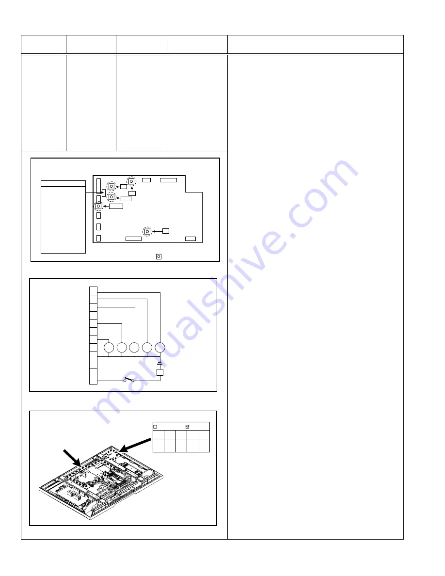
Vs VR:170V ADJ
(R9424)
Vset VR:160V ADJ
(R9640)
Ve VR:155V ADJ
(R9646)
Va VR:70V ADJ
(R9219)
Vscan VR:-60V ADJ
(R9628)
DC voltmeter
Signal generator
Resistor (1k
Ω
)
DC power
supply
4.6 ADJUSTMENT PROCEDURE
Connector
CN0C4
[MAIN POWER
PWB]
Vs
Vset
Ve
Va
Vscan
CAUTION:
•
During adjustment operation of PDP POWER VOLTAGE,
don't touch the heat sink of the MAIN POWER PWB. If you
touch it, electric shock may be caused.
< When MAIN POWER PWB is not replaced >
(1) Connect the DC voltmeter, load resistor (1k
Ω
), DC
power supply and switch SW1 to the CN0C4 connector
and turn on the main power and switch SW1. (See
Fig.2)
(2) Adjust Vs (170V ADJ) VR, Vset (160V ADJ) VR, Ve (155V
ADJ) VR, Va (70V ADJ) VR and Vscan (-60V ADJ) VR so
that the Vs, Vset, Ve, Va and Vscan voltage coincides
with the values in the voltage label.
(3) Input a PAL all-black signal and check that it coincides
with the values in the voltage label.
(4) Readjust if the adjusted value is different from those
in the voltage label.
NOTE:
•
Designed value for the panel is printed on a label on the
upper-right at the back of the PDP. (See Fig.3)
< When MAIN POWER PWB is replaced >
CAUTION:
•
Before making adjustments, be sure not to turn on the
power when the CN8002, CN8003, CN8005, CN8006
and CN8008 connectors are connected, as this may
cause the PDP to break down.
(1) Disconnect the CN8002, CN8003, CN8005, CN8006
and CN8008 connectors on the MAIN POWER PWB.
(2) Connect the DC voltmeter, load resistor (1k
Ω
), DC
power supply and switch SW1 to the CN0C4 connector
and turn on the main power and switch SW1. (See
Fig.2)
(3) Adjust Vs (170V ADJ) VR, Vset (160V ADJ) VR, Ve (155V
ADJ) VR, Va (70V ADJ) VR and Vscan (-60V ADJ) VR so
that the Vs, Vset, Ve, Va and Vscan voltage coincides
with the values in the voltage label.
(4) Turn off the main power and switch SW1, and connect
the CN8002, CN8003, CN8005, CN8006 and CN8008
connectors and turn on the power again.
(5) Input a PAL all-black signal and check that it coincides
with the values in the voltage label.
(6) If the adjusted value is different from those in the
voltage label, fine-tune without unplugging the
connectors.
CAUTION:
•
Designated power supply voltage of the panel (Vs, Vset,
Ve, Va, Vscan) varies according to the PDP unit.
•
Pay careful attention during adjustment, as any error in
procedure may cause the PDP to break down.
CN0C4
Fig. 1
Voltage adjustment VR
MAIN POWER PWB voltage adjustment point
1 : Vs
2 : Vset
3 : Ve
4 : NC
5 : Va
6 : NC
7 : Vscan
8 : NC
9 : GND
10 : POWER
11 : PANEL POWER
12 : Vs_ON
Vscan
Vset
Vs
Va
Ve
1
2
3
4
5
6
7
8
9
10
11
12
Vs
Vset
Ve
NC
Va
NC
Vscan
NC
GND
POWER
PANEL POWER
Vs_ON
SW1
Vscan
Va
Ve
Vset
Vs
3.3V ~ 5.0V
(DC power supply)
1k
Ω
(Resistor)
Fig. 2
CN0C4
Fig. 3
NTSC
Va
XX
XX
XX
XX
XX
Ve
Vset
Vsc
Vs
NTSC/PAL
Voltage label
MAIN POWER PWB


