PD-42DX
1-40 (No.52088)
3.8 ADJUSTMENT PROCEDURE
3.8.1 DISPLAY UNIT
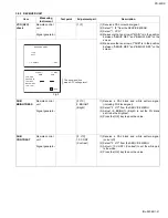
Item
Measuring
instrument
Test point
Adjustment part
Description
PDP POWER
SUPPLY
VOLTAGE
DC voltmeter
Signal generator
Resistor (5
Ω
/5W)
Connector
CN0C4
[PDP POWER
PWB]
Vs VR :170V ADJ
(R628)
Vd VR : 60V ADJ
(R721)
<When PDP POWER PWB is not replaced>
(1) Connect the load resistor (5
Ω
/5W) to the CN0C4
connector on the PDP POWER PWB. (See Fig.1)
(2) Adjust Vs (170V ADJ) VR and Vd (60V ADJ) VR
such that the Vs and Vd load resistor voltage tally
with those in the table.
(3) Ensure that the voltage between pins 5 and 6 of
CN0C4 (5V) coincides with the table's value.
(4) Input a PAL (625i) all-black signal and check that
voltage coincides with the values in the table.
(5) Readjust if the adjusted value is different from those
in the table.
NOTE:
Designated value for the panel is printed on a small
label on the top left corner at the back of the PDP.
<When PDP POWER PWB is replaced>
CAUTION:
Before making adjustments, be sure not to turn on the
power when the CN0AT and CN0AU connectors are
connected, as this may cause the PDP to break down.
(1) Disconnect the CN0AT and CN0AU connectors on
the PDP POWER PWB.
(2) Connect the load resistor (5
Ω
/5W) to the CN0C4
connector and turn on the power.
(3) Adjust Vs (170V ADJ) VR and Vd (60V ADJ) VR so
that the Vs and Vd voltage coincides with the values
in the table.
(4) Ensure that the voltage between pins 5 and 6 of
CN0C4 (5V) coincides with the values in the table.
(5) Turn off the power, and connect the CN0AT and
CN0AU connectors and turn on the power again.
(6) Input a PAL (625i) all-black signal and check that it
coincides with the values in the table.
(7) If the adjusted value is different from those in the
table, fine-tune without unplugging the connectors.
CAUTION:
Designated power supply voltage of the panel (Vs, Vd)
varies according to the PDP unit. (See Fig.2)
Pay careful attention during adjustment, as any error in
procedure may cause the PDP to break down.
Fig.1
Fig.2
Item
measured
CN0AU/CN0AT
Disconnected
CN0AU/CN0AT
Connected
Adjustment
VR
Vs
R628
Vd
R721
5V
5.25 ± 0.15V
5.20 ± 0.15V
-
Designated
value for panel
±0.5V
Designated
value for panel
±0.5V
Designated
value for panel
±0.5V
Designated
value for panel
±0.5V
CN0C4
1
2
3
4
5
6
5
Ω
/5W
/5W
(Load resistor)
(Load resistor)
Vd
Vs
5V
Vs
NC
Vd
NC
5V
GND
㧔
PDP POWER PWB: Chassis base
㧕
CN0AU
CN0AT
Chassis
Chassis
Base
Base
R628
Voltage adjustment VR (Vs, Vd)
Voltage adjustment VR (Vs, Vd)
SYSTEM POWER
SYSTEM POWER
PWB
PWB
AUDIO
AUDIO
PWB
PWB
LINE FILTER PWB
LINE FILTER PWB
Display Input
Display Input
Terminal
Terminal
Designated panel voltage
Designated panel voltage
Vs/Vd voltage label
Vs/Vd voltage label
CN0C4
Connector for
Connector for
adjustment
adjustment
Fig.1
Fig.1
PDP POWER PWB
PDP POWER PWB
DISPLAY INTERFACE PWB
DISPLAY INTERFACE PWB
Designated value for panel / layout of adjustment VR
Designated value for panel / layout of adjustment VR
(Rear view)
(Rear view)
170V
ޓ#&,
R721
60V
ޓ#&,
㧗
㧗
Summary of Contents for PD-42DX
Page 47: ...PD 42DX No 52088 1 47 ...

