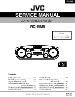


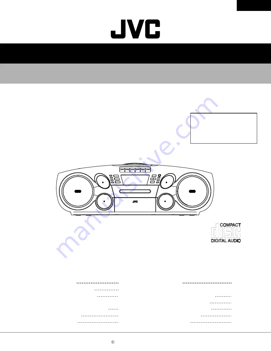
RC-BM5
No.21129
Oct. 2002
COPYRIGHT 2002 VICTOR COMPANY OF JAPAN, LTD.
SERVICE MANUAL
Contents
Safety precautions
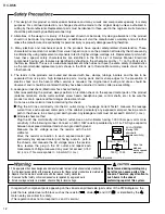
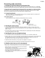
Preventing static electricity
Important for laser products
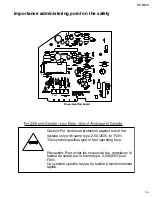
Importance administering point
on the safety
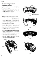
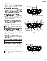
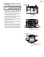
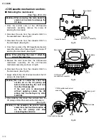
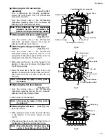
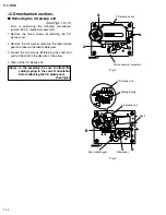
Disassembly method
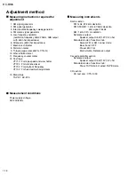
Adjustment method
1-2
1-3
1-4
1-5
1-6
1-16
RC-BM5
Area suffix
J ----------------------------- U.S.A.
C -------------------------- Canada
Trouble shooting
Flow of functional operation
until TOC read
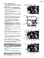
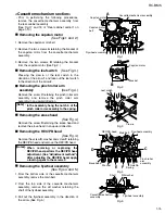
Maintenance of laser pickup
Replacement of laser pickup
Description of major ICs
Wiring connection
1-19
1-20
1-21
1-21
1-22
1-37
CD PORTABLE SYSTEM
Summary of Contents for RC-BM5
Page 41: ...RC BM5 2 1 A B C D E F G 1 2 3 4 5 Block diagram ...
Page 48: ...RC BM5 2 8 RC BM5 H A B C D E F G 1 2 3 4 5 Printed circuit boards Main board Reverse side ...
Page 49: ...RC BM5 2 9 A B C 1 2 3 4 5 Tuner board Cassette board Reverse side Reverse side ...
Page 50: ...RC BM5 2 10 A B C D 1 2 3 4 5 Display board Reverse side Power amplifier board Reverse side ...
Page 51: ...RC BM5 2 11 A B C 1 2 3 4 5 Volume switch board Reverse side Phone jack board Reverse side ...