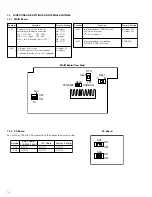
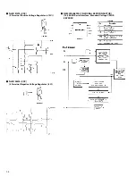
1-5
Turn this VR and confirm that data varies between 0 and 255.
Turning clockwise should increase the value.
This VR also controls the LCD contrast. It is Normal at the
center. Turning the VR clockwise should increase contrast
and counter-clockwise should decrease it. The LCD back light
should be OFF at the most clockwise position.
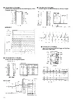
Turn this VR and confirm that data varies between 0 and 255.
Turning it clockwise should increase the value.
This VR also controls the SC FINE data output.
Turn this VR and confirm that data varies between 0 and 255.
Turning it clockwise should increase the value.
This VR also controls the LENGTH HF data output
Turn this VR and confirm that data varies between 0 and 255.
Turning it clockwise should increase the value.
This VR also controls the LENGTH Y data output
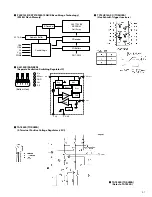
Turn this JOG and confirm that data is switched to 5M, 20M,
50M and 100M. Turning it clockwise should increase the
value.
The initial value when the unit is turned ON is 20M.
This JOG also checks the JOG rotation and JOG hardware
when LENGTH is selected in addition to SHUTTER JOG
check.
Turn JOG and confirm that data is switched to 0
°
, 90
°
, 180
°
and 270
°
. Turning clockwise should increase the value.
The initial value when the unit is turned ON is 0
°
.
This JOG also checks the JOG rotation and JOG hardware
when SC COARSE is selected in addition to V.GAIN JOG
check.
Operate this SW and confirm that A, B and PRE are displayed
correctly when the SW is in the corresponding position.
This SW should also vary ASPECT internally: When A (16:9),
B (Letter Box) and PRE (4:3) are displayed, the internal mode
should vary accordingly.
Operate this SW and confirm that LOW, MID and HIGH are
displayed correctly when the SW is in the corresponding
position.
This SW should also vary the supply voltage to the camera
internally: When LOW (15 V), MID (17 V) and HIGH (19 V) are
displayed, the internal voltage should vary accordingly.
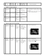
When the unit is
turned ON, 15 V is
output regardless
of the position of
this SW, until this
SW is changed to
another position.
Set each SW to ON and OFF and confirm that the
corresponding display changes to H (ON) or L (OFF).
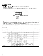
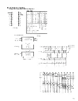
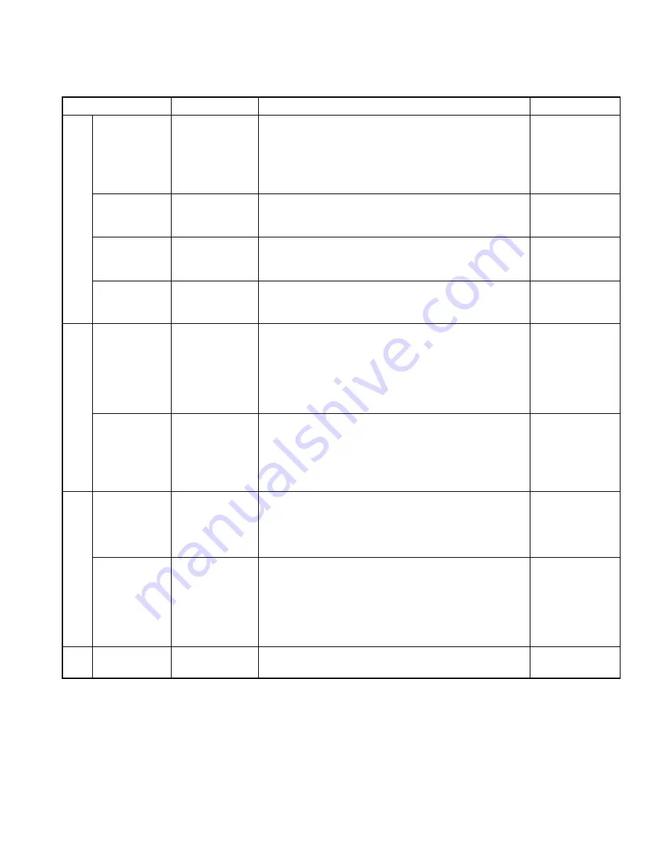
IRIS
128
M.BLACK (SC FINE)
128
WHITE Bch(C)
128
WHITE Rch(Y)
128
SHUT JOG(LENGTH)
20M
V.GAIN JOG(SC)
0
°
W.BAL(ASPECT)
PRE(4:3)
GAIN(VOLT)
LOW(15V)
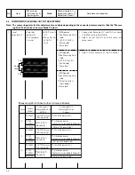
DIP SW12345678
LLLLLLLLL
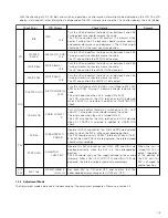
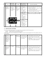
Check Point
Check Details
LCD Display
Remark
VR
JOG
SW
DIP
SW
IRIS
MASTER
BLACK
WHITE Bch
WHITE Rch
SHUTTER JOG
V.GAIN JOG
W.BAL
STEP GAIN
SW 1 to 8
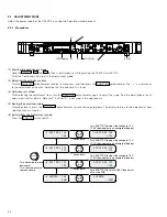
With the checking of VR, JOG dials and switches, operating a control causes information to be displayed on the LCD. The LCD
display is retained until other information is displayed on the LCD. However, pressing the CALL button displays the initial display.
1.3.4
Adjustment Mode
The Adjustment mode is detailed in the description of the adjustment procedures. Please see section 2.2.