1-11
RX-7000RBK
No.
1
2
3
4
5
6
7
8
9
10
11
12
13
14
15
16
17
18
19
20
21
22
23
24
25
26
27
28
29
30
31
32
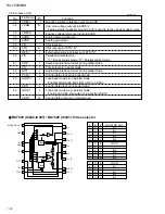
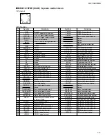
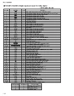
Pin name
SDOS
OCKS
MIS
BICK
LRCK
SDTI1
SDTI2
SDTI3
SDTO
DAUX
DFS
DEM1
DEM0
MCKO
DVDD
DVSS
PD
XTS
ICKS1
ICKS0
CAD1
CAD0
LOUT3
ROUT3
LOUT2
ROUT2
LOUT1
ROUT1
LIN-
LIN+
RIN-
RIN+
SDTO Source select pin
"L" : Internal ADC output, "H" : DAUX input
ORed with serial control register if P/S="L".
MCKO Clock frequency select pin
"L" : MCLK, "H" : MCLK/2. ORed with serial control register if P/S= "L".
Connect to GND
Audio serial data clock pin
Input/Output channel clock pin
DAC1 Audio serial data input pin
DAC2 Audio serial data input pin
DAC3 Audio serial data input pin
Audio serial data output pin
AUX Audio serial data input pin
Double speed sampling mode pin
"L" : Normal speed, "H" : Double speed, the ADC is powered down.
ORed with serial control register if P/S="L".
De-emphasis pin
ORed with serial control register if P/S="L"
De-emphasis Pin
ORed with serial control register if P/S="L"
Master clock output pin
Digital power supply pin
Digital ground pin
Power-down & Reset pin
When "L", the AK4527 is powered-down and the control registers are reset
to default state. If the state of CAD0-1 changes, then the AK4527
must be reset by PDN.
X'tal oscillator Select/Test mode pin
"H" : X'tal Oscillator selected
"L" : External clock source selected
Input clock select 1 pin
Input clock select 0 pin
Chip address pin
Used during the serial control mode.
Chip address pin
Used during the serial control mode.
Lch #3 analog output pin
Rch #3 analog output pin
Lch #2 analog output pin
Rch #2 analog output pin
Lch #2 analog output pin
Rch #1 analog output pin
Lch analog negative Input Pin
Lch analog positive Input Pin
Rch analog negative Input Pin
Rch analog positive Input Pin
Function
AK4527(1/2)
I/O
I
I
I
I
I/O
I
I
I
O
I
I
I
I
O
-
-
I
I
I
I
I
I
O
O
O
O
O
O
I
I
I
I
3. Pin function (1/2)
Summary of Contents for RX-7000RBK
Page 26: ...1 26 RX 7000RBK MEMO ...
Page 44: ...RX 7000RBK 3 2 MEMO ...


