RX-8012VSL/RX-8010VBK
1-21
PIN
1
2
3
4
5
6
7
8
9
10
11
12
13
14
15
16
17
18
19
20
21
22
23
24
25
26
27
28
Symbol
XTI
V
DD
C
DGNDC
V
DD
DGND
D+
D-
V
BUS
DGNDU
PLYBCK
SSPND
ZERO
TEST3
TEST2
TEST1
TEST0
VccR
AGNDR
V
OUT
R
AGND
V
COM
Vcc
V
OUT
L
AGNDL
VccL
AGNDP
VccP
XTO
I/O
IN
-
-
-
-
I/O
I/O
IN
-
OUT
OUT
OUT
IN
IN
IN
IN
-
-
OUT
-
-
-
OUT
-
-
-
-
OUT
Function
Crystal Oscillator Input.
Digital Power Supply for Clock Generator, +3.3V.
Digital Ground for Clock Generator.
Digital Power Supply, +3.3V.
Digital Ground.
USB Differential Input/Output Plus.
USB Differential Input/Output Minus.
USB Bus Power (This pin NEVER consumes the USB bus power).
Digital Ground for USB Transceiver.
Playback flag, active LOW. (LOW: playback, HIGH: idle).
Suspend flag, active LOW. (LOW: suspend, HIGH: operational).
Zero flag, (LOW: Normal, HIGH: ZERO).
Test pin 3. Connect to digital ground.
Test pin 2. Connect to digital ground.
Test pin 1. Connect to digital ground.
Test pin 0. Connect to digital ground.
Analog Supply for R-channel, +5V.
Analog Ground for R-channel.
Analog Output for R-channel.
Analog Ground.
Common for DAC.
Analog Supply, +5V.
Analog output for L-channel.
Analog Ground for L-channel.
Analog Supply for L-channel, +5V.
Analog Ground for PLL.
Analog Supply for PLL, +5V.
Crystal Oscillator Output.
Note:
(1) 3.3V tolerant.
(2) Schmitt trigger input with internal pull-down, 5V tolerant.
3.Pin function
1.Pin layout
1
2
3
4
5
6
7
8
9
10
11
12
13
14
28
27
26
25
24
23
22
21
20
19
18
17
16
15
XTI
V
DD
C
DGNDC
V
DD
DGND
D+
D-
V
BUS
DGND
PLYBCK
SSPND
ZERO
TEST3
TEST2
XTO
VccP
AGNDP
VccL
AGNDL
V
OUT
L
Vcc
V
COM
AGND
V
OUT
R
AGNDR
VccR
TEST0
TEST1
(1)
(2)
(2)
(2)
(2)
(2)
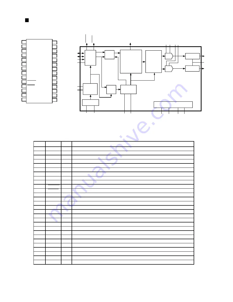
PCM2702E-X (IC410) : Digital/ Analog converter
USB I/F
8x
Oversampling
Digital Filter
Multi-level
Delta-Sigma
Modulator
USB clock
generator
Crystal OSC
Power supply
DAC
DAC
Low-pass
Filter
Low-pass
Filter
D+
D-
VBUS
DGNDU
VDDC
DGNDC
XTI
XTO
VCC
AGND
VDD DGND
VOUTL
VOUTR
ZER
O
FIFO
SPACT
Audio clock
generator
VCOM
System Clock
audio
data
USB packet
data
WRCLK
MCLK
RDCLK
VDDP DGNDP
PL
YBCK
SSPDN
VccL
A
GNDL
VccR
A
GNDR
2. Block diagram


