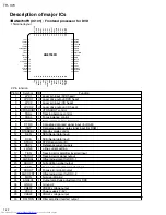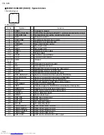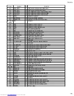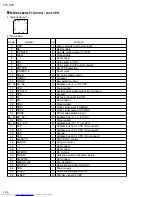
TH-V70
1-36
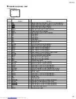
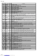
100
101
102
103
104
105
106
107
108
109
110
111
112
113
114
115
116
117
118
119
120
121
122
123
124
125
126 - 131
132
133,134
135
136 - 139
140
141 - 144
145
146
147
148 - 153
154
155
156
157,158
159
160
161
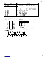
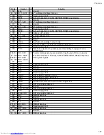
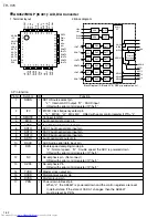
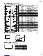
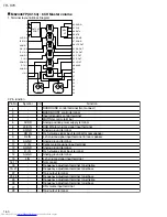
OSCVss
OSCVdd
MVCKVdd
SCEN
MVCKVss
ACLKVss
SCMD
ACLKVdd
Vdddak
Vssdac
Cr/R
IOM
C/Cb/B
Vaa3
Y/G
Vssa
VREF
Vaa
CVBS/C
RSET
COMP
Vss
VCLK
VSYNC
HSYNC
Vddio
VIO7 - VIO2
Vssio
VIO1,VIO0
Vdd
AD31 - AD28
Vddio
AD27 - AD24
PWE3-
AD23
Vssio
AD22 - AD17
Vddio
AD16
PWE2-
AD15,AD14
Vdd
SCLK
ACK
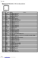
-
-
-
I
-
-
I
-
-
-
O
O
O
-
O
-
-
-
O
O
O
-
-
-
-
-
-
-
-
-
I/O
-
I/O
I/O
I/O
-
I/O
-
I/O
I/O
I/O
-
O
I/O
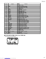
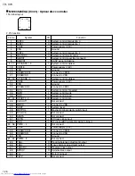
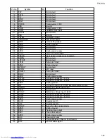
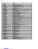
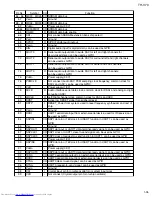
Function
I/O
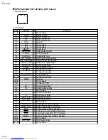
Pin No.
Symbol
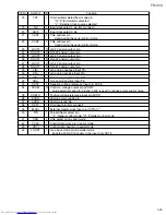
Oscillator ground
Oscillator power supply (1.8V)
Main and video clock PLL power supply (3.3V)
Scan chain test enable
Main and video clock PLL ground
Audio clock PLL ground
Scan chain test mode
Audio clock PLL power supply (3.3V)
DAC digital power supply (1.8V)
DAC digital ground
Video DAC3 output (A second composite video; Cr output for composite, Cr
output for component, Red output for SCART
Cascaded DAC differential output used to dump current into external resistor
for power
Video DAC2 output (Chrominance output for NTSC/PAL S-Video; Cb output
for component, Blue output for SCART
DAC analog power supply (3.3V)
Video DAC1 output (Luminance for S-Video and component, G output for
SCART)
DAC analog ground
Not connect (Input voltage reference (1.2V typical) for output DACs)
Connect to power supply (1.8V)
Video DAC output (Composite video; Chrominance output for S-Video)
Current setting resistor of output DACs
Compensation capacitor connection
Ground
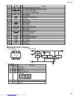
Not connect (VCLK input/output for video I/O port function
Not connect (Bi-directional HSYNC signal for devices that do not use end
active video/start active video (EAV/SAV) codes; can be used as GPIO)
Not connect (Bi-directional VSYNC signal for devices that do not use end
active video/start active video (EAV/SAV) codes; can be used as GPIO)
Power supply (3.3V)
Not connect (Bi-directional digital video port data bus; can be used as GPIO)
Ground
Not connect (Bi-directional digital video port data bus; can be used as GPIO)
Power supply (1.8V)
P multiplexed address/data bus
Power supply (3.3V)
P multiplexed address/data bus
Byte write enable for FLASH, EEPROM, SRAM or peripherals
P multiplexed address/data bus
Ground
P multiplexed address/data bus
Power supply (3.3V)
P multiplexed address/data bus
Byte write enable for FLASH, EEPROM,SRAM or peripherals
P multiplexed address/data bus
Power supply (1.8V)
External bus clock used for programmable host bus peripherals
Programmable WAIT-/ACK-/RDY- control
Summary of Contents for TH-V70
Page 55: ...TH V70 1 55 M E M O ...

