TH-V70
1-51
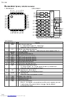
29
30
31
32
33
34
35
36
37
38
39
40
41
42
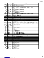
-
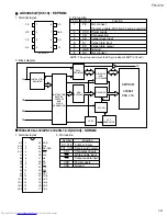
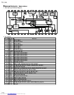
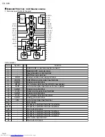
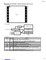
AVSS
L OUT
R OUT
C OUT
RL OUT
RR OUT
LFE OUT
AGND
DGND
STB
DATA
CLK
DVDD
-
-
O
O
O
O
O
O
-
-
I
I
I
-
L/R volume input terminal
Analog negative power supply terminal
L ch output
R ch output
Center volume signal output terminal
L ch volume signal output terminal for rear speaker
R ch volume signal output terminal for rear speaker
SUB Woofer volume signal output terminal
Analog ground terminal
Digital ground terminal
Latch input terminal
Volume data input terminal
Clock input terminal for data transfer
Digital power supply terminal
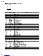
Pin No.
Symbol
I/O
Function
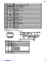
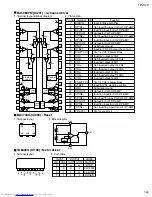
1. Terminal layout
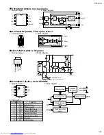
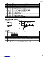
MM1613DN (IC402) : Regulator
2. Block diagram
1
(TOP VIEW)
2
3
5
4
3. Pin function
Cont
GND
Cn
Vout
Vin
1
2
3
4
5
Pin No. Symbol
Function
ON/OFF Control pin
Cont Vo
H ON
L OFF
Cont pin must be connected with V
IN
pin, if it is not used.
Ground
Noise decrease pin, Connecting 0.01uF capacitor can decrease output noise.
If the noise decrease capacitor is not connected, the pin may be influenced by outside noise.
Output pin, The capacitor must be connected with output pin more than 1uF.
Input pin
The capacitor is required to connect with input pin more than 1uF.
Bias
Driver
Current
limiter
Thermal
shutdown
Reference
GND
Vin
Cont
Cn
Vout
5
1
2
3
4
Summary of Contents for TH-V70
Page 55: ...TH V70 1 55 M E M O ...

