background image

TH-V70

1-9

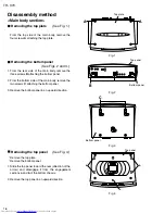
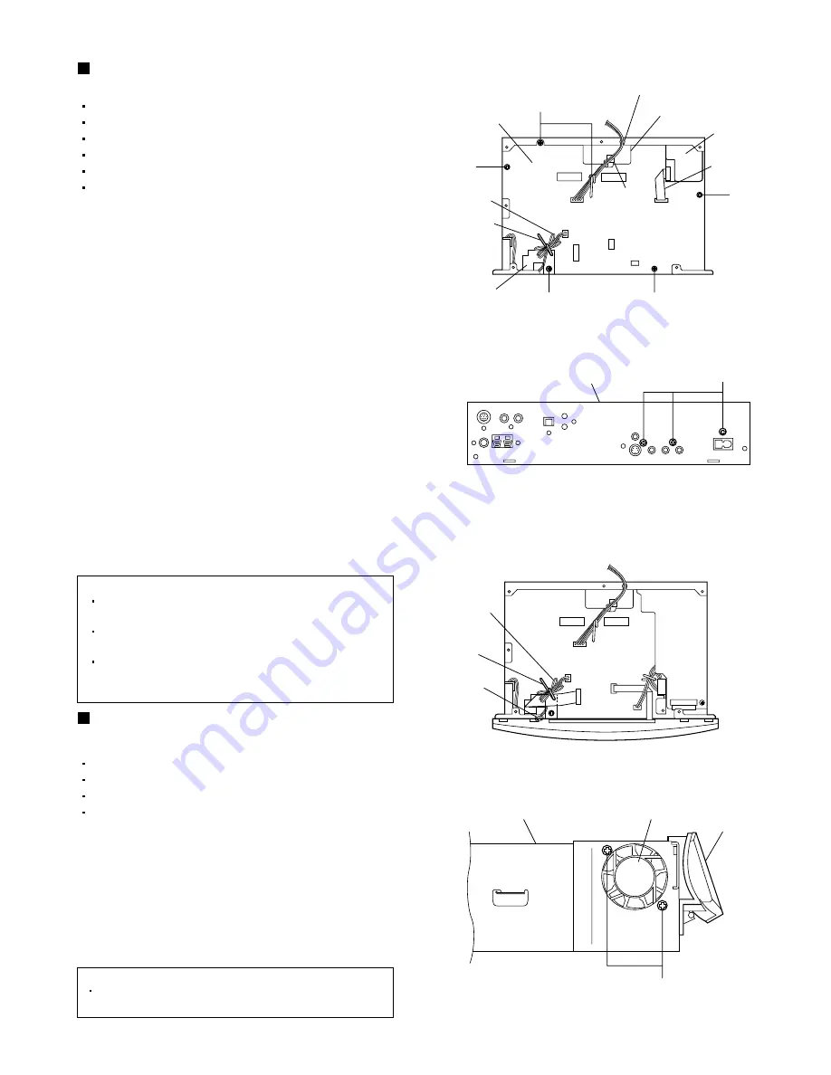
Fig.11

Fig.12

Fig.13

Fig.14

Wire holder

Main board

CN592

M

M

M

M'

Wire clamp

Bottom chassis

Fan motor

Front panel
assembly

M

CN972

CN972

CN805

Rear panel

N

P

Tuner

Compulink board

Insert this wire into the notch.

Tie band

Wire clamp

Fan motor wire

Fan motor wire

Card wire

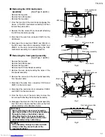
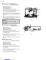
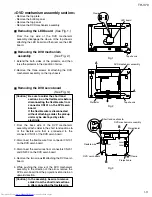
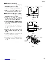
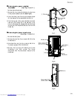
Removing the main board


(See Figs. 11 and 12.)

1.

2.

3.

4.

5.

6.

7.

Disconnect the card wire from connector CN805 on 
the main board.

Remove the wire clamp bundling the fan motor wire 
and then disconnect the wire from connector 
CN972 on the main board.

Disconnect the card wire from connector CN592 on 
the compulink board.

Remove the five screws 

M

 and screw 

M'

 attaching 

the main board.

From the rear side of the main body, remove the 
three screws 

N

 attaching the main board.

Remove the rear panel with the tuner and 
compulink board.

Take out the main board from the bottom chassis.

Remove the top plate.
Remove the bottom panel.
Remove the top panel.
Remove the DVD mechanism assembly.
Remove the front panel assembly.
Remove the DSP/Audio board.

[Reference]  Attaching the main board
    When attaching the screw M', attach the wire 
    holder together with it.
    After connecting the wires to the connectors, 
    bundle them using the wire clamp.
    Insert the DVD mechanism assembly wire 
    into the notch on the bottom chassis.
                                                           (See Fig. 11.)

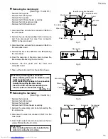
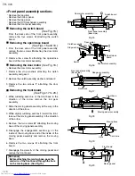
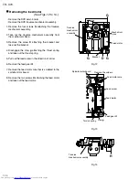
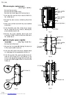
Removing the fan motor


(See Figs. 13 and 14.)

1.

2.

3.

Remove the wire clamp and tie band bundling the 
fan motor wire.

Disconnect the wire from connector CN972 on the 
main board.

From the left side of the main body, remove the two 
screws 

P

 attaching the fan motor.

Remove the top plate.
Remove the bottom panel.
Remove the top panel.
Remove the DVD mechanism assembly.

[Reference]
   After mounting the fan motor, bundle the fan 
   motor wire using the wire clamp.

Summary of Contents for TH-V70

Page 1: ...recautions Preventing static electricity Importance administering point on the safety 1 2 1 3 1 4 1 6 1 21 1 22 54 Disassembly method Adjustment method Description of major ICs TH V70 Area suffix J U S A C Canada DVD DIGITAL THEATER SYSTEM SP PWV70 XV THV70 SP XCV70 SP XSV70 SP XSV70 SP XSV70 SP XSV70 ...

Page 2: ...uct antenna terminals knobs metal cabinet screw heads headphone jack control shafts etc to be sure the product is safe to operate without danger of electrical shock Do not use a line isolation transformer during this check Plug the AC line cord directly into the AC outlet Using a Leakage Current Tester measure the leakage current from each exposed metal parts of the cabinet particularly any expose...

Page 3: ...on prevention by static electricity Ground the workbench by laying conductive material such as a conductive sheet or an iron plate over it before placing the traverse unit optical pickup on it 2 1 Ground the workbench 2 2 Ground yourself Use an anti static wrist strap to release any static electricity built up in your body In order to maintain quality during transport and before installation both ...

Page 4: ...inued protection against risk of fire replace only with same type 1 6A 125V for F901 This symbol specifies type of fast operating fuse Precaution Pour eviter risques de feux remplacez le fusible de surete de F901 comme le meme type que 1 6A 125V Ce sont des fusibles suretes qui functionnes rapide F901 ...

Page 5: ...place only with same type 4A 125V for F403 8A 125V for F504 8A 125V for F505 This symbol specifies type of fast operating fuse Precaution Pour eviter risques de feux remplacez le fusible de surete de F403 comme le meme type que 4A 125V F504 comme le meme type que 8A 125 et 8A 125V pour F505 Ce sont des fusibles suretes qui functionnes rapide ...

Page 6: ...and 3 1 2 3 From the rear side of the main body remove the three screws B attaching the bottom panel From the bottom side of the main body remove the two screws C attaching the bottom panel Remove the bottom panel in an upward direction 1 2 Slide the top panel toward the rear direction of the arrow and disengage it from the engagement sections a and b of the bottom chassis Remove the top panel in ...

Page 7: ... 7 and 8 1 2 3 4 5 6 Remove the wire clamp bundling the wires of the front panel assembly Remove the card wire of the front panel assembly from the wire holder Disconnect the wires from connectors CN106 and CN814 on the main board Disconnect the card wires from connectors CN802 and CN813 on the main board From the front side of the main body remove the two screws F attaching the front panel assemb...

Page 8: ... the bottom chassis Remove the top plate Remove the bottom panel Remove the top panel Remove the DVD mechanism assembly Remove the top plate Remove the bottom panel Remove the top panel Remove the DVD mechanism assembly Removing the DSP Audio board See Figs 9 and 10 1 2 3 From the top side of the main body remove a screw G attaching the DSP Audio board From the rear side of the main body remove th...

Page 9: ... panel with the tuner and compulink board Take out the main board from the bottom chassis Remove the top plate Remove the bottom panel Remove the top panel Remove the DVD mechanism assembly Remove the front panel assembly Remove the DSP Audio board Reference Attaching the main board When attaching the screw M attach the wire holder together with it After connecting the wires to the connectors bund...

Page 10: ...t panel assembly remove the two screws R attaching the door motor assembly Remove the screw S attaching the open close board of the door motor assembly Removing the open close board See Figs 15 and 16 Removing the door motor See Fig 16 1 2 3 4 5 6 7 While widening section e of the front base in the direction of the arrow remove the rod gear assembly Slide the moving panel assembly all the way in t...

Page 11: ...panel Remove the DVD mechanism assembly Removing the DVD mechanism assembly See Fig 2 Removing the DVD servo board See Fig 3 Caution In the assembly be sure to remove solder from the short land sections b after connecting the flexible wire 1 2 3 4 5 From the back side of the DVD mechanism assembly attach solder to the short land sections b of the flexible wire that is connected to the connector CN...

Page 12: ...verse mechanism assembly and then take out the DVD traverse mechanism assembly Removing the DVD pickup unit See Figs 5 to 7 1 2 3 4 5 6 Remove the DVD servo board Remove the DVD traverse mechanism assembly From the top side of the DVD traverse mechanism assembly remove the screw D attaching the bracket Remove the claw g attaching the thrust spring and then take out the torsion spring Remove the le...

Page 13: ...the DVD traverse mechanism assembly Slide the DVD pickup unit all the way in the direction of the arrow Mesh the lead screw to the section k of DVD pickup unit and then set the end of the lead screw to the section h Attach the thrust spring See Fig 6 Attach the bracket See Fig 5 Reference Refer to the explanation of Removing the DVD pickup unit on the preceding page Removing the spindle motor boar...

Page 14: ...e the DVD traverse mechanism assembly Remove the four screws G attaching the traverse mechanism assembly Take out the traverse mechanism assembly from the mechanism base Remove the screw D attaching the bracket and take out the bracket Disengage the claw g attaching the thrust spring and take out the thrust spring Pull out the lead screw in the direction of arrow Remove the feed gear M Remove the ...

Page 15: ...he DVD mechanism assembly From the back side of the DVD mechanism assembly disconnect the card wire from connector CN202 on the DVD servo board See Fig 3 From the top side of the CD mechanism assembly remove the two screws K attaching the clamper base assembly Disconnect the wire from connector CN101 on the switch board while lifting the clamper base assembly slightly and remove the clamper base a...

Page 16: ...f the speaker main body remove the four screws A attaching the heat sink cover and then remove the heat sink cover Remove the eight screws B attaching the amplifier assembly Move the amplifier assembly backward and disconnect the wire from connector CN109 in the lower part of the amplifier assembly 1 2 Pull out the knob Remove the ten screws C ten screws D and screw E attaching the rear panel Remo...

Page 17: ...t Disconnect the pre amplifier board from the connector CN201 on the mother board and take out the pre amplifier board Pull out the push button Remove the two screws G and nut attaching the volume bracket Remove the rear panel Removing the power supply SP terminal board See Figs 4 and 5 1 2 3 4 Remove the two screws H attaching the AC bracket Disconnect the power supply SP terminal board from the ...

Page 18: ...oard A B From the bottom side of the mother board remove the two screws K and two screws L attaching the power amplifier board A B Remove the power amplifier board A B from connectors CN202 CN203 CN205 and CN206 on the mother board Remove the rear panel Remove the pre amplifier board Remove the power supply SP terminal board Removing the power amplifier board A See Figs 9 and 10 1 2 3 Remove the f...

Page 19: ...terminal board Remove the four screws P attaching the power transformer and then remove the power transformer from the transformer bracket of the mold base Removing the power amplifier board B See Figs 9 and 11 1 2 3 Remove the four screws N attaching the heat sink to the power amplifier board B See Fig 9 From the bottom side of the power amplifier board B disengage the four engagement sections c ...

Page 20: ...ody and the ornament panel the section indicated by the arrows and lift the net little by little to remove Note To prevent damaging the ornament panel and speaker main body insert cushioning plates etc above and below the tip of the flat bladed screwdriver or a similar tool 2 3 From the back side of the ornament panel remove the two screws Q attaching the LED indicator Disconnect the wire from con...

Page 21: ...TOP button fourth button from left and EJECT farthest right button button on the main unit plug in the power FL indication TEST E Monitor indication Upper left of the monitor E Europe Pressing the PAUSE button fifth button from right Initialization starts FL indication ATT will appear Initialization is complete Set the power to standby Make sure that the panel has closed Pull out the power plug ...

Page 22: ...t supply J line current setting Tracking error amplifier inverted input Tracking error signal output Offset adjustment for DRC 1 Full addition signal output Focus error amplifier inverted input Focus error signal output Offset adjustment for DRC 2 Not use Monitor Output amplitude adjustment for DRC Ground 2 VREF2 voltage output Power supply 2 5V VHALF voltage output Filter amplifier inverted outpu...

Page 23: ...nvelope detection filter AGC amplifier gain control AGC amplifier level control TEST signal input RF signal positive input RF signal inverted input Internal four partition CD RF input 1 Internal four partition CD RF input 2 Internal four partition CD RF input 3 Internal four partition CD RF input 4 External two partition DVD RF input 2 External two partition DVD RF input 1 Power supply 1 5V VREF1 ...

Page 24: ...ding mechanism photo switch Slide door lock detection AD Area discrimination signal Key input1 AD Key input2 AD Reference power supply Power supply Oscillator output 8MHz Oscillator input 8MHz Ground Not used Connect to ground Not used Not connect PANECON serial communication data output MP3 JPEG mode H for DVD disc PANECON serial communication clock Serial communication data output for PANTERA Se...

Page 25: ...nd Slide door motor control 0 Slide door motor control 1 Slide door motor speed control AC switching detection Headphone input detection System power supply control DVD power supply control TUNER power supply control RDS communication data RDS communication clock Not used IF DATA and tuner receive detection Not used TUNER serial communication data output TUNER serial communication clock TUNER seri...

Page 26: ...1 Write enable Not connect Chip select for ODC Chip select for ZIVA Not connect HD TYPE selection Driver mute SP motor brake control LSI reset Bus selection input Address bus 0 3 for CPU Power supply System clock signal output Not connect Ground Not use Connect to VSS Not connect Power supply Clock signal input 13 5MHz Clock signal output 13 5MHz CPU mode selection input Address bus 4 11 for CPU P...

Page 27: ...ROM data input EEPROM data output Power supply Communication clock Communication input data Communication output data Clock for ADSC serial Connect to VSS ADSC serial data output Not use Connect to ground Not use Connect to ground Not use Connect to ground Interrupt input of ADSC Interrupt input of ODC Interrupt input of ZIVA Interrupt input of SODC Interruption of system control Address data sele...

Page 28: ... initializing System control address Power supply 1 8V Ground Connect to VDD18 Connect to VSS System control address Power supply 3 3V Ground Connect to VDD3 System control chip select System control write System control read System control data Not connect Connect to VSS System reset Master terminal polarity switch input Not connect Not connect Off track signal input RF dropout BCA data of making...

Page 29: ...ignal for track cross formation Not connect Not connect Pull up to VHALF Analog ground Not connect HPF input Pull up to VHALF Not connect Analog power supply Connect to capacitor 2 for PLL Connect to capacitor 1 for PLL Analog ground Connect to resistor for VREF reference current source Reference voltage input 2 2V Not connect Reference voltage input 1 65V Connect to capacitor 2 for DSL Connect to...

Page 30: ...ost chip select ATAPI host chip select ATAPI host address ATAPI host address ATAPI slave master diagnosis input ATAPI host address ATAPI output of selection of host data bus width Not connect ATAPI host interruption output ATAPI host DMA response Power supply 3 3V Ground ATAPI host ready output Not connect ATAPI host read ATAPI host write ATAPI host DMA request Not connect ATAPI host data 15 0 14 ...

Page 31: ... input 2 Flag input 3 Interruption input Digital ground LR clock input A for audio interface Bit clock input A for audio interface Data output 0 for audio interface Data output 1 for audio interface Data output 2 for audio interface Data output 3 for audio interface Not connect LR clock input B for audio interface Bit clock input B for audio interface Data input 0 for audio interface Data input 1 ...

Page 32: ... external SRAM Data I O 5 for external SRAM Data I O 4 for external SRAM Data I O 3 for external SRAM Data I O 2 for external SRAM Data I O 1 for external SRAM Data I O 0 for external SRAM Digital ground Address output 0 for external SRAM Address output 1 for external SRAM Address output 2 for external SRAM Address output 3 for external SRAM Address output 4 for external SRAM Address output 5 for ...

Page 33: ...illator output Crystal oscillator input Digital power supply 74LCX373MTC IC512 IC513 Octal D type latch 1 Terminal layout 2 Truth table 1 OE 2 Q0 3 D0 4 D1 5 Q1 6 Q2 7 20 19 18 17 16 15 14 D2 VCC Q7 D7 D6 Q6 Q5 D5 TOP VIEW 8 D3 9 Q3 10 GND 13 12 11 D4 Q4 LE OE H L L L Y Z Qn L H INPUTS OUTPUT LE X L H H D X X L H X Don t care Z High impedance Qn Q outputs are latched at the time when the LE input ...

Page 34: ... I O I O I O I O Power supply 3 3V SDRAM data bus Power supply 1 8V SDRAM data bus Ground SDRAM data bus Power supply 3 3V SDRAM data byte enable SDRAM address bus Ground SDRAM address bus Ground SDRAM address bus Power supply 3 3V SDRAM address bus SDRAM clock Ground SDRAM clock enable SDRAM address bus Power supply 3 3V SDRAM address bus Not connect SDRAM address bus Ground SDRAM address bus res...

Page 35: ... sampling clock frequency common clock for DACs and ADC can be used as GPIO Power supply 1 8V Audio interface serial data clock common clock for DACs and analog to digital converter ADC Left Right channel clock common clock for DACs and ADC Active low RESET signal for peripheral reset RESET_Power from system used to reset frequency synthesizer and rest of chip Ground UART1 serial data input from e...

Page 36: ...ART DAC analog power supply 3 3V Video DAC1 output Luminance for S Video and component G output for SCART DAC analog ground Not connect Input voltage reference 1 2V typical for output DACs Connect to power supply 1 8V Video DAC output Composite video Chrominance output for S Video Current setting resistor of output DACs Compensation capacitor connection Ground Not connect VCLK input output for vid...

Page 37: ...ltiplexed address data bus Ground P multiplexed address data bus Power supply 3 3V Byte write enable for FLASH EEPROM SRAM or peripherals Address latch enable Latched address 3 0 Ground Read Bus hold acknowledge in slave mode Bus hold request from external master in slave mode Power supply 1 8V Peripheral chip select 0 generally used for enabling the program store ROM FLASH Programmable general pu...

Page 38: ...ect pin Ground Not connect Not connect Reset input Data request signal VCO lock input Digital data input DSP format status signal DSP channel status signal Data error output signal Reset signal input Analog power supply Connect to ground Connect to ground Filter selection Connect to ground Ground Not connect Connect to VDD Digital signal input Digital signal output Not connect DSP control signal D...

Page 39: ...nect Power supply Not connect Not connect Analog test tone output Not connect Not connect Digital out mute output System mute output Not connect Optical Coaxial switching Optical Coaxial switching Not connect Not connect Test pin Not connect Symbol Function I O 1 Terminal layout MM1563DF IC407 Regulator 2 Block diagram 1 TOP VIEW 2 3 4 7 5 6 GND Vin Thermal shutdown Bias Cont Driver Current limite...

Page 40: ...iver communication CS INITIAL Not connect VDD B5V 8MHz main clock output 8MHz main clock input Ground Not connect Ground Reference voltage Not connect FL reset input POWER LED switching signal KEY LED switching signal POWER LED switching signal KEY LED switching signal Remote control receiver switching signal Not connect Ground POWER LED DIMMER switching signal KEY LED DIMMER switching signal Not ...

Page 41: ...8 Pin No Symbol Function Not connect Program enable With built in pull up resistor Power supply Chip selection Cereal clock input Cereal data input Cereal data output Ground Not connect A0 A16 I O1 I O8 CS1 WE OE VDD VSS Address inputs Data inputs outputs Chip select inputs Write enable input Output enable input Power supply Ground Symbol Function NC A16 A14 A12 A7 A6 A5 A4 A3 A2 A1 A0 I O1 I O2 I...

Page 42: ... pin L Internal ADC output H DAUX input ORed with serial control register if P S L MCKO Clock frequency select pin L MCLK H MCLK 2 ORed with serial control register if P S L Connect to GND Audio serial data clock pin Input Output channel clock pin DAC1 Audio serial data input pin DAC2 Audio serial data input pin DAC3 Audio serial data input pin Audio serial data output pin AUX Audio serial data in...

Page 43: ...sitive Input Pin Rch analog negative Input Pin Rch analog positive Input Pin Negative voltage reference Input pin AVSS Common voltage output pin AVDD 2 Large external capacitor around 2 2uF is used to reduce power supply noise Positive voltage reference input pin AVDD Analog power supply pin Analog ground pin X tal input pin Not connect External master clock input pin if XTS L Parallel Serial sele...

Page 44: ...UT2 IN2 IN2 8 7 6 5 OUT1 IN1 IN1 VEE 1 2 3 4 2 IN1 3 IN1 4 VEE 5 IN2 6 IN2 7 OUT2 8 VCC 1 Terminal layout BA3121 IC100 IC101 IC102 Ground isolation amplifier VCC OUT2 VM2 IN2 8 7 6 5 OUT1 VM1 IN1 GND 1 2 3 4 2 Block diagram 1 8 6 VCC OUT1 VM2 7 OUT2 R R R R R R R R 3 IN1 2 VM1 5 IN2 4 GND 1 I O 1 O I 1 O I 2 I O 2 C2 C3 VSS 1 Terminal layout Block diagram BU4066BCF IC151 Quad analog witch 2 3 4 5 ...

Page 45: ...rol Vcc for CH1 2 power block Inverted output of CH2 Non inverted outpur of CH2 Inverted output of CH1 Non inverted outpur of CH1 Non inverted output of CH4 Inverted output of CH4 Non inverted output of CH3 Inverted output of CH3 Vcc for CH3 4 power block Input for Ch4 stand by control Substrate ground Output for CH3 OP AMP Inverting input for CH3 OP AMP Non inverting input for CH3 OP AMP Output f...

Page 46: ... compensating capacitor Short brake terminal FG3 phase synthesizing signal output terminal Not connect Rotation detecting terminal Not connect Reference terminal for output voltage control Output terminal for output voltage control Power save terminal FG signal output terminal Power supply terminal Gain switching terminal Power supply terminal for motor Connecting terminal for output current detec...

Page 47: ... CS SK NC GND DO DI 1 2 3 4 8 7 6 5 Top view Memory array Data register Mode decode logic Clock generator circuit Output buffer Address decoder VCC GND DO DI CS SK 2 Pin function PE VCC CS SK DI DO GND NC 1 2 3 4 5 6 7 8 Pin No Symbol Function Not connect Power supply Chip select input Serial clock input Serial data input Serial data output Ground Not connect OUTPUT DIVIDERS 7 bit P 11bit Q 7 bit ...

Page 48: ... enabling all inputs except CLK CKE and DQM Selects bank to be activated during row address latch time Selects bank for read write during column address latch time Row column addresses are multiplexed on the same pins Row address RA0 RA10 Column address CA0 CA7 Ground for the input buffers and core logic Masks system clock to freeze operation from the next cycle CKE should be enabled at least one ...

Page 49: ...n Selection of a kind of component LPF Component signal Cb input or baseband signal Selecting amplifier gain for component signal Component signal Cr input or baseband signal Capacitor terminal for regulator 2drive 1drive select for component signal Component signal Cr output Component signal Cb output Brightness signal output Brightness signal output DC voltage output Not connect Chrominance sign...

Page 50: ...S BOOST control terminal Input attenuator control terminal MUTING control terminal Analog positive power supply terminal SUB Woofer volume signal input terminal Analog ground terminal R ch volume signal input terminal for rear speaker L ch volume signal input terminal for rear speaker Analog ground terminal Center volume signal input terminal Analog ground terminal R ch volume signal input termina...

Page 51: ...nal for data transfer Digital power supply terminal Pin No Symbol I O Function 1 Terminal layout MM1613DN IC402 Regulator 2 Block diagram 1 TOP VIEW 2 3 5 4 3 Pin function Cont GND Cn Vout Vin 1 2 3 4 5 Pin No Symbol Function ON OFF Control pin Cont Vo H ON L OFF Cont pin must be connected with VIN pin if it is not used Ground Noise decrease pin Connecting 0 01uF capacitor can decrease output nois...

Page 52: ...Terminal layout NJM78M05FA IC805 IC953 Regulator 1 INPUT 2 GND 3 OUTPUT 2 Block diagram 1 1 IN 2 OUT 3 GND 4 CTRL 4 2 3 1 Terminal layout PQ05RD21 IC951 Regulator 2 Block diagram Specific IC 1 4 2 3 2 3 AMP AGC Detector BPF I V conversion PD Vcc Comp 22k ohm magnetic shield VDD OUT GND for trimming circuit RPM6938 SV4 IC711 IC871 Remote control receiver 1 Block diagram 3 1 2 ...

Page 53: ... A0 X Decoder 1 9 16 25 48 10 12 15 47 11 26 27 46 28 29 36 38 45 37 A19 A0 NC WE CE VSS OE D15 D0 VCC Address inputs To provide memory addresses During Sector Erase A19 A11 address lines will select the sector During Block Erase A19 A15 address line will select the block No connection Unconnected pins Write Enable To control the Write operations Chip Enable To activate the device when CE is low G...

Page 54: ...H1 NF CH1 VE CH2 VE CH2 VE PRE Vcc CH2 NF CH2 IN CH1 IN CH1 NF PRE Vcc CH1 VE CH1 VE CH2 VE CH2 VE PRE Vcc CH2 NF CH2 IN CH3 IN CH3 NF CH3 VE CH3 VE 2 Block diagram 1 Terminal layout STK404 130 IC105 Power amplifier STR 12 3 45 VIN 4 START REG T S D O V P LATCH O S C DRIVE Vth 1 Comp 1 Vth 2 Comp 2 GND 3 OCP FB 5 S 2 D 1 2 Block diagram 1 Terminal layout STR G6651 IC901 Switching regulator 1 2 3 4...

Page 55: ...TH V70 1 55 M E M O ...
Page 56: ...TH V70 VICTOR COMPANY OF JAPAN LIMITED AUDIO COMMUNICATION BUSINESS DIVISION PERSONAL MOBILE NETWORK BUSINESS UNIT 10 1 1Chome Ohwatari machi maebashi city 371 8543 Japan 200207 No 21089 ...

Reviews: