background image

2-5

UX-V30

I

H

A

B

C

D

E

F

G

1

2

3

4

5

6

Tuner circuit (UX-V30)

FM/TUNER MAIN SIGNAL
AM SIGNAL

Summary of Contents for UX-V30

Page 1: ... of major ICs 1 2 1 3 1 4 1 14 1 18 1 19 1 19 1 20 Area Suffix This service manual is printed on 100 recycled paper UF China AUTO REVERSE AUT O T A PE SELECT O R T APE DOWN UP MULTI CONTROL TAPE FM AM CD STANDBY ON PHONES MD AUX REC REV MODE AHB PRO TIMER CLOCK VERTICAL DISC LOADING MECHANISM COMPACT DIGITAL AUDIO VOLUME CD OPEN CLOSE REMOTE CONTROL RM RXUV5R DIMMER SLEEP DISPLAY FM MODE MD AUX AH...

Page 2: ...urrnet check Electrical shock hazard testing After re assembling the product always perform an isolation check on the exposed metal parts of the product antenna terminals knobs metal cabinet screw heads headphone jack control shafts etc to be sure the product is safe to operate without danger of electrical shock Do not use a line isolation transformer during this check Plug the AC line cord direct...

Page 3: ...fety switches malfunction the laser is able to function 6 CAUTION Use of controls adjustments or performance of procedures other than those specified herein may result in hazardous radiation exposure VARNING Osynlig laserstrålning är denna del är öppnad och spårren är urkopplad Betrakta ej strålen VARO Avattaessa ja suojalukitus ohitettaessa olet alttiina näkymättömälle lasersäteilylle Älä katso s...

Page 4: ...inal then remove the rear cover backward with releasing the hooks 1 2 3 Disassembly method Main body Removing the rear cover See Fig 1 and 2 Prior to performing the following procedure remove the rear cover Move the side panels in the direction of the arrow and remove them backward 1 Removing the side panels See Fig 3 and 4 Fig 1 Fig 2 Fig 3 Fig 4 Rear cover A A A A A Rear cover B B Side panel L S...

Page 5: ...onnect the card wire from connector CN303 and the harness from CN306 and CN307 on the main board respectively Disconnect the harness from connector CN902 on the power transformer Remove the screw E attaching the main board on the right side of the body Remove the screw F and the two screws G attaching the heat sink on the back of the body 1 2 3 4 Disconnect connector CN301 and CN302 on the main bo...

Page 6: ...front panel assembly toward the front 1 2 3 Removing the front panel assembly See Fig 10 to 12 Prior to performing the following procedure remove the rear cover the side panels the cassette mechanism assembly the main board and the front panel assembly Remove the plastic rivet attaching the head phone board and release the joint d 1 Removing the head phone board See Fig 13 Fig 9 Fig 10 Fig 11 Fig ...

Page 7: ... Disconnect the harness from connector CN901 on the AC supply board Remove the four screws I attaching the power transformer 1 2 3 Removing the power transformer See Fig 15 Prior to performing the following procedure remove the rear cover the side panels and the cassette mechanism assembly Disconnect the harness from connector CN901 on the AC supply board Remove the screw F attaching the heat sink...

Page 8: ...ess the eject button on the front side of the cassette mechanism assembly to open the cassette door Remove the four screws L attaching the cassette mechanism assembly on the back of the assembly 1 2 Removing the cassette mechanism assembly See Fig 16 and 17 Prior to performing the following procedure remove the rear cover the side panels and the cassette mechanism assembly Fig 16 Fig 17 Opt Dig ou...

Page 9: ...and the harness from CN605 on the CD servo control board Remove the CD mechanism assembly from the CD mechanism cover by pulling out it from the three bosses h 1 2 3 4 5 6 Front panel assembly Removing the CD mechanism assembly See Fig 18 to 21 Remove the screw O attaching the LED board A 1 Removing the LED board A See Fig 21 Prior to performing the following procedure remove the rear cover the si...

Page 10: ...CD servo control board in the direction of the arrow by releasing the two joints j 1 2 Removing the CD servo control board See Fig 22 Remove the belt and the two screws R attaching the loading motor on the back of the front panel assembly 1 Removing the loading motor See Fig 18 Prior to performing the following procedure remove the CD mechanism cover CD mechanism assembly Remove the two screws S a...

Page 11: ...raser head 7 Loosen the reversing azimuth screw retaining the Playback Recording Eraser head 8 Take out the Playback Recording Eraser head from the front of the head mount 9 The Playback Recoring Eraser head should also be removed similarly according to Steps 1 8 above Reassembling the Playback Recording Eraser Head 1 Reassemble the playback head from the front of the head mount to the position as...

Page 12: ... screws 2 retaining the main motor assembly See Fig 4 4a 2 While raising the main motor remove the capstan belt from the motor pulley See Fig 4a Caution 1 Be sure to handle the capstan belt so carefully that this belt will not be stained by grease and other foreign matter Moreover this belt should be hanged while referring to the capstan belt hanging method in Fig 5 6 Fig 4a Main motor assembly Ca...

Page 13: ... pull out the flywheel R and L respectively from behind the cassette mechanism Removing the Reel Pulse P C board and Solenoid See Fig 9 1 Remove the five pails d h reataining the reel pulse P C board 2 From the surface of the reel pulse P C board parts remove the two pawls i and j retaining the solenoid Flywheel R Flywheel L Capstan shaft R Capstan shaft L Slit washer Slit washer Fig 8 Flywheel R ...

Page 14: ... Center Adjustment of main volume to reference output VOL 28 Precautions for measurement 1 Apply 30pF and 33k to the IF sweeper output side and 0 082 F and 100k in series to the sweeper input side 2 The IF sweeper output level should be made as low as possible within the adjustable range 3 Since the IF sweeper is a fixed device there is no need to adjust this sweeper 4 Since a ceramic oscillator i...

Page 15: ... Position Cassette mechanism section Cassette mechanism section Back side Front panel assembly section Head azimuth adjusting screw Reverse side Head azimuth adjusting screw Forward side Playback Recording eraser head Head azimuth adjusting screw Forward side Head azimuth adjusting screw Reverse side ...

Page 16: ...ly when the head has been changed Test tape VT712 3kHz Measurement output terminal Headphone terminal When the test tape VT712 3kHz has been played back with the recording and playback mechanism at the beginning of forward winding the frequency counter reading of the difference between both of the mechanism should be 6 0Hz or less Adjust VR37 so that the frequency counter reading becomes 2 940 3 0...

Page 17: ...e recording and pausing condition in advance 2 While repetitively inputting the reference frequency signal of 1kHz and 10kHz from OSC IN record and playback the rape 3 While recording and playback the test tape in TYPE adjust VR31 for Lch and VR32 for Rch so that the output deviation between 1kHz and 10kHz becomes 1dB 2dB 1 While recording and playback mechanism load the test tapes AC 514 to TYPE ...

Page 18: ...matic measurement of TE amplitude and automatic tuning of TE balance 500mv div 2ms div Fig 1 Approx 3sec pin 25 of IC601 TE Approx 1 8V VREF Tracking error waveform at TOC reading Power ON Power Key Confirm that the Focus error S cuve siganl at the pin27 of IC601 is approx 2Vp p Confirm that the siganl from pin24 IC603 is 0V as a accelerated pulse during approx 400ms Confirm the waveform of the Tr...

Page 19: ...the life of the laser diode has expired the following symptoms wil appear 1 The level of RF output EFM output ampli tude of eye pattern will below Is RF output 1 1 0 15Vp p Replace it NO YES O K 3 Semi fixed resistor on the APC PC board The semi fixed resistor on the APC printed circuit board which is attached to the pickup is used to adjust the laser power Since this adjustment should be performe...

Page 20: ...L AMP 1 input pin BTL AMP 1 input pin For gain adjustment BTL AMP 1 input pin Non inverting side BTL AMP 1 input pin Inverting side BTL AMP 2 input pin Inverting side BTL AMP 2 input pin Non inverting side BTL AMP 2 input pin For gain adjustment BTL AMP 2 input pin External transistor collector PNP connection 5V power supply output External transistor PNP base connection Reset output Reset output ...

Page 21: ...K MDATA DSL PLL VCO AVDD2 SUB CODE BUFFER SSEL SQCK SUBQ AVDD2 CLVS CRC BLKCK CLDCK SBCK SUBC DEMPH RESY FLAG6 RESY EFM DEMODULATION SUBCODE DEMODULATION SYNC INTERPOLATION 16k SRAM CIRC ERROR CORRECTION DEINTERLEVE LRCKIN MSEL BCLK SSEL SRDATAIN PSEL IOSEL DIGITAL DEEMPHSIS 8TIMES OVER SAMPUNC DIGITAL FILTER 1BIT DAC LOGIC S PEM R PEM L DIGITAL AUDIO INTERFASE DIGITAL AUDIO INTERFASE INTER POLATI...

Page 22: ...al output Kick pulse output Tracking drive output Focus drive output Reference voltage input pin for D A output block TVD FOD FBA TBAL Focus Balance adjust signal output Tracking Balance adjust signal output Focus error signal input Analog input Tracking error signal input Analog input RF envelope signal input Analog input Vibration detect signal input H detect Off track signal input H off track T...

Page 23: ...A 12 CS BDO 13 BDO 14 CS BRT 15 OFTR 16 NRFDET 17 GND 18 36 PDAC 35 PDBD 34 PDF 33 PDE 32 PDER 31 PDFR 30 TBAL 29 FBAL 28 EF 27 EF OUT 26 TE 25 TE OUT 24 CROSS 23 TE BPF 22 VDET 21 LD OFF 20 VREF 19 ENV 30 24 25 26 23 22 1 4 3 33 32 34 31 36 35 13 14 15 16 20 2 21 6 29 7 28 27 8 9 10 17 11 12 19 ENV CURCUIT RF DET AGC EQ BDO OFTR VCBA VCBA VCBA VCBA ...

Page 24: ...ction terminal ARF output terminal RF detection capacity connection terminal HPF amp capacity connection terminal Capacity connection terminal for RF discernment side envelope detection BDO output terminal Capacity connection terminal for RF discernment side envelope detection OFTR output terminal RFDET output terminal Connect to GND 3TENV output terminal VREF output terminal APC OFF control termi...

Page 25: ...tion USDATA USCK UQRIN UNC USQCK ICVSS UX2 UX1 VDD UXT1 UXT2 URESET UREM URDSCK UJOG1 UBEAT2 UBEAT1 U BCTL UXRESET UMCLK UMDATA UMLD UPBMUTE ULATCH UREEL UFAUX UAVSS USAFEYCD 29 30 31 32 33 34 35 36 37 38 39 40 41 42 43 44 45 46 47 48 49 50 I I I I I I I I O I O I O O O O O O O O O I RESET CLOSE switch Abnormal voltage detection 1 Abnormal voltage detection 2 Body key input 1 Body key input 0 Tape...

Page 26: ... AM OSC REG AM RF AFC AM AGC O I O I I I AM Local oscillation Signal output This is a terminal of AM Local oscillation circuit Register value between pin 26 and pin28 besides the frequency width of the input signal AM RF signal input This is an output terminal of voltage for FM AFC This is an AGC voltage input terminal for AM O O I O AM detection output FM detection output Mpx input terminal O O I...

Page 27: ...utput port Input output port Data input output Function IF counter signal input IF signal output Not use AM Local OSC signal output FM Local OSC signal input Power suplly VDD 4 5 5 5V When power ON Reset circuit move PLL charge pump output H Local OSC frequency Height than Reference frequency L Low Agreement Height impedance Input for active lowpassfilter of PLL Output for active lowpassfilter of ...

Page 28: ... DATA CLOCK Q1 Q2 Q3 Q4 Vss Vdd OUTPUT ENABLE Q5 Q6 Q7 Q8 Q s Qs 1 2 3 4 5 6 7 8 16 15 14 13 12 11 10 9 1 Pin layout 8 STAGE SHIFT REGISTER 8 BIT LATHES 3 STATE OUTPUTS 1 2 3 15 Q1 Q8 10 9 DATA CLOCK STROBE OUTPUT ENABLE PARALLEL OUTPUT Q s Qs SERIAL OUTPUT 2 Block diagram BU4094BCF X IC304 IC303 Serial to parallel port extension ...

Page 29: ... Limiter Integrator Comparator Demodulator 1 2 3 4 5 6 7 8 9 10 GND OUT1 P1 VZ IN1 IN2 VCC1 VCC2 P2 OUT2 Input Output Mode IN1 IN2 OUT1 OUT2 Brake 0 0 0 0 1 0 1 0 0 1 0 1 1 1 0 0 CLOCKWISE COUNTER CLOCKWISE Brake LB1641 IC501 DC Motor Driver 1 Pin Layout 2 Pin Functions ...

Page 30: ...yback amplifier input R1 R2 I Playback amplifier input NF2 Playback amplifier negative feedback OUT2 Playback amplifier output EQ2 I Equlaizer CTL2 I Pre Amplifier input swithing time constant RIN2 I Recording amplifier input RNF2 I Recording amplifier negative feedback ROUT2 O Recording amplifier output O LC I ALC low cut LPF I ALC low pass filter GND I Vcc Power supply RF I Repple filter EQCTL E...

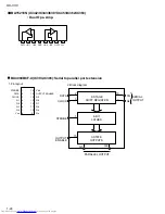
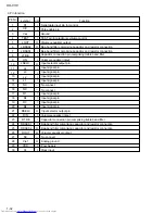
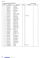
Page 31: ...1 31 UX V30 LC75342 ...

Page 32: ...or connection pin comprising treble band filter LIN Volume equalizer intput LSEL0 Input selector output pin L4 Input signal pin L3 Input signal pin L2 Input signal pin L1 Input signal pin NC No connect NC No connect R1 Input signal pin R2 R3 R4 I I I Input signal pin Input signal pin Input signal pin RSEL0 Input selector output pin RIN Volume equalizer intput RTRE Capacitor connection pin comprisi...

Page 33: ...EF MPXIN Vdda Vssa FLOUT CIN TEST XOUT XIN Vssd Vddd MODE RST RDDA RDCL RDS ID READY I O O O O O O I I I I I I I O Reference voltage output Vdda 2 Baseband multiplexed signal input Analog power supply 5V Analog ground Subcarrier input comparator input Subcarrier input filter output Test input Crystal oscillator input exeternal reference input Crystal oscillator output 4 332MHz Digtal ground Digtal...

Page 34: ...1 34 UX V30 MEMO ...

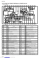
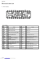
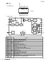
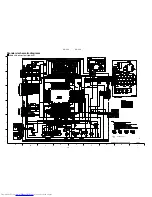
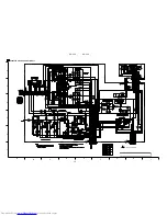
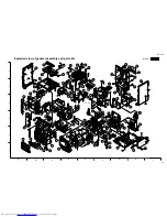
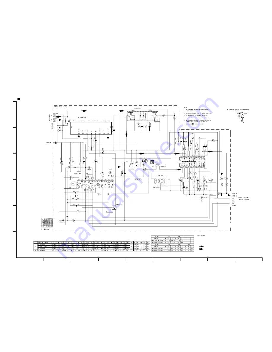
Page 35: ...2 1 UX V30 I H A B C D E F G 1 2 3 4 5 6 Block diagram ...

Page 36: ...2 2 I H A B C D E F G 1 2 3 4 5 6 UX V30 UX V30 Standard schematic diagrams CPU LCD driver circuit UX V30 TUNER SIGNAL micom_V30 00 2 4 9 53 Create by Kops ...

Page 37: ...2 3 UX V30 I H A B C D E F G 1 2 3 4 5 6 CD SIGNAL cd_mp_v30 00 2 4 9 42 Create by Kops CD servo circuit UX V30 ...

Page 38: ... V30 UX V30 Parts are safety assurance parts When replacing those parts make sure to use the specified one CD SIGNAL TAPE P B SIGNAL TUNER SIGNAL AUX IN SIGNAL MAIN SIGNAL 30main1 00 2 4 9 27 Create by Kops Power amplifier circuit UX V30 ...

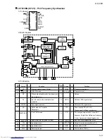
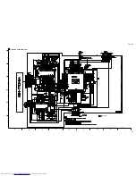
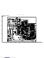
Page 39: ...2 5 UX V30 I H A B C D E F G 1 2 3 4 5 6 Tuner circuit UX V30 FM TUNER MAIN SIGNAL AM SIGNAL ...

Page 40: ...5 6K MA3051 M TX VMC0163 R09 QGB2011M1 10 0 033 VMC0163 R10 BU4094BCF FA1A4ZX 330P 1K 0 033 12K 1K 1K 5 6K 33K QVPA603 503AZ 12K 100 VWS304 06A13K 330P QQR0620 001 BA3126N 1 2K 3 9K 1 8K 12K QVPA603 103AZM 3 3K 2SB562 C 4 7K FA1F4MX 2 2K FA1A4ZX 1 8K AN7317 FA1A4ZX 2 2K 2SC2001 K 0 0012 0 0012 470K 2SC1623 6 X 2SC1623 6 X 2SC1623 6 X 2SC1623 6 X 2SC1623 6 X 33K 2SC1623 6 X MA152WA TX 2 2K 2 2K FA1...

Page 41: ... supply circuit FS V30 Parts are safety assurance parts When replacing those parts make sure to use the specified one 0 00 2 4 9 55 Create by Kops Parts are safety assurance parts When replacing those parts make sure to use the specified one trans30 00 2 4 9 55 Create by Kops ...

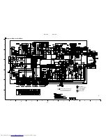
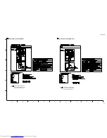
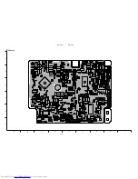
Page 42: ...2 8 I H A B C D E F G 1 2 3 4 5 6 UX V30 UX V30 Printed circuit boards Main board ...

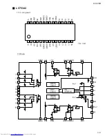
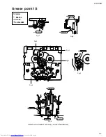
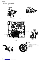
Page 43: ...2 9 UX V30 I H A B C D E F G 1 2 3 4 5 6 Micon P C board ...

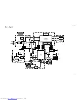
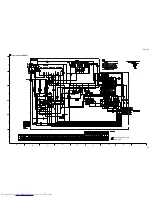
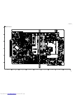
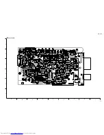
Page 44: ...2 10 I H A B C D E F G 1 2 3 4 5 6 UX V30 UX V30 CD board ...

Page 45: ...2 11 UX V30 I H A B C D E F G 1 2 3 4 5 6 Tuner P W B ...

Page 46: ...2 12 I H A B C D E F G 1 2 3 4 5 6 UX V30 UX V30 MEMO ...

Page 47: ...its assemblies are not available as service parts Contents Exploded view of general assembly and parts list Cassette mechanism and parts list Electrical parts list Packing materials and accessories parts list UX V30 3 3 3 5 3 10 3 21 UF China Area suffix ...

Page 48: ...UX V30 3 2 MEMO ...

Page 49: ... 52 53 54 55 56 57 58 59 60 84 61 74 75 76 61 44 82 79 62 67 68 68 70 71 71 72 78 69 69 69 69 66 63 31 32 33 34 35 35 36 37 38 39 40 32 16 18 19 20 22 24 25 29 30 30 30 30 41 42 43 21 17 23 28 28 26 28 79 21 2 3 59 Exploded view of general assembly and parts list Block No M M M 1 27 32 30 15 Main board 86 CD Servo board Tuner board 30 61 83 ...

Page 50: ...412 0908DJ FFC WIRE 1 TU TO FMB 41 QUQ412 1022CJ FFC WIRE 1 CD TO MAIN 42 QUQ412 1320CJ FFC WIRE 1 CD TO FMB 43 QUQ110 1607BJ FFC WIRE 1 PICKUP TO CD 44 GV40111 001A PROTECT SHEET 1 45 GV10022 001A TOP COVER 1 46 GV20047 001A CASSETTE DOOR 1 47 GV40074 001A CASSETTE LENS 1 48 VYH7366 001MM GEAR 1 General assembly Item Parts number Parts name Area A Parts list Q ty Description Block No M1MM 49 GV40...

Page 51: ...UX V30 3 5 Cassette switch board Head amplifier mechanism control board 63 C C SLC S1YPM Cassette mechanism assembly and parts list Block No M M M 2 ...

Page 52: ...KW5300 002 PIN ROL SP L 1 26 VKW5285 001 RETURN SPRING 1 27 VKY3149 002 CASSETTE SP 1 28 VKM3906 002 PLAY SW LEVER 1 29 VKS1166 003 CONTROL CAM 1 30 VKW5279 001 HEAD BASE SP R 1 31 VKW5280 001 HEAD BASE SP L 1 32 VKS5603 00D MAIN PULLEY ASY 1 33 VKS3785 001MM FR ARM 1 34 VKW5284 002 SWING SPRING 1 35 VKS2278 003 TRIGGER ARM 1 36 VKW5301 001 FR SPRING 1 37 VKW5266 001 ELEVATOR SPRING 1 38 WDL214025...

Page 53: ...V30 3 7 Fig 1 EM 30L Fig 2 EM 30L EM 30L Fig 3 EM 30L Fig 4 EM 30L EM 30L EM 30L EM 30L Fig 1 Fig 2 Fig 3 Fig 4 Remove the Head mount Ass y on the Chasis Base Grease point 1 3 EM 30L UD 24 LEN 320M Grease ...

Page 54: ...5 Fig 1 Fig 2 EM 30L EM 30L Fig 5 Fig 1 Fig 2 EM 30L Fig 3 Fig 3 Fig 4 EM 30L Fig 4 LEN 320M Grease point 2 3 Note It is a putting up of the control cam to UD 24H Hanarl and LEN 320M Grease dipping on the Control cam ...

Page 55: ...UX V30 3 9 Fig 1 EM 30L EM 30L EM 30L EM 30L Fig 2 Fig 4 Fig 6 Fig 3 Fig 5 EM 30L EM 30L UD 24 UD 24 Fig 1 Fig 6 Fig 2 Fig 5 Fig 4 Fig 3 Grease point 3 3 ...

Page 56: ...20 25V C2600 QCBB1HK 221Y C CAPACITOR 220PF 10 50V C2700 QCBB1HK 221Y C CAPACITOR 220PF 10 50V C2800 QETN1EM 475Z E CAPACITOR 4 7MF 20 25V C3100 QETM1EM 828 E CAPACITOR A 8200MF 20 25V C3101 QFLM1HJ 104Z MF CAPACITOR 10MF 5 50V C3102 EEKC1AM 107ZJC E CAPACITOR C3103 QETN1CM 107Z E CAPACITOR 100MF 20 16V C3104 QETC1AM 336Z E CAPACITOR 33MF 20 10V C3105 QETN1HM 225Z E CAPACITOR 2 2MF 20 50V C3150 QE...

Page 57: ...Y C RESISTOR 2 7K 5 1 4W R1505 QRE141J 272Y C RESISTOR 2 7K 5 1 4W R1600 QRE141J 303Y C RESISTOR 30K 5 1 4W R1601 QRE141J 303Y C RESISTOR 30K 5 1 4W R1700 QRE141J 221Y C RESISTOR 220 5 1 4W R1701 QRE141J 562Y C RESISTOR 5 6K 5 1 4W R1702 QRE141J 103Y C RESISTOR 10K 5 1 4W R1800 QRE141J 912Y C RESISTOR 9 1K 5 1 4W R1801 QRE141J 272Y C RESISTOR 2 7K 5 1 4W R1802 QRE141J 222Y C RESISTOR 2 2K 5 1 4W R...

Page 58: ...F RES I M 5 6 1 0W R9201 QRE141J 103Y C RESISTOR 10K 5 1 4W R9202 QRE141J 103Y C RESISTOR 10K 5 1 4W R9203 QRE141J 820Y C RESISTOR 82 5 1 4W R9301 QUY150 050Y C RESISTOR 4 7K 5 1 4W R9302 QRE141J 333Y C RESISTOR 33K 5 1 4W R9303 QRE141J 101Y C RESISTOR 1 0K 5 1 4W R9304 QRE141J 390Y C RESISTOR 39 5 1 4W R9403 QRE141J 100Y C RESISTOR 10 5 1 4W R9404 QRE141J 6R8Y C RESISTOR 6 8 5 1 4W R9405 QRE141J ...

Page 59: ... 1C T2 ZENER DIODE BACK UP CONT D7091 1SS133 T2 SI DIODE US5V D7092 1SS133 T2 SI DIODE 5V REMCON STBLE D8001 1SS133 T2 SI DIODE D8002 SLR 342VC T LED D8003 SLR 342MC T LED D8201 SELU1E56BM LED D8202 SELU1E56BM LED D8205 MTZJ10C T2 Z DIODE I M D8206 MTZJ10C T2 Z DIODE I M D8601 1SS133 T2 SI DIODE D8602 1SS133 T2 SI DIODE D8603 1SS133 T2 SI DIODE IC701 UPD78064GF 172 IC SYSTEM MICOM IC703 KIA78S06P ...

Page 60: ...RESISTOR R8001 NRSA02J 102X MG RESISTOR R8002 NRSA02J 102X MG RESISTOR R8003 NRSA02J 122X MG RESISTOR R8005 NRSA02J 473X M G RESISTOR R8011 NRSA02J 102X MG RESISTOR R8012 NRSA02J 102X MG RESISTOR R8013 NRSA02J 122X MG RESISTOR R8014 NRSA02J 152X MG RESISTOR R8015 NRSA02J 222X MG RESISTOR R8016 NRSA02J 272X MG RESISTOR R8017 NRSA02J 392X MG RESISTOR R8018 NRSA02J 562X MG RESISTOR R8019 NRSA02J 103X...

Page 61: ...X C CAPACITOR C6099 NCS21HJ 391X C CAPACITOR C6154 NCS21HJ 151X C CAPACITOR C6156 NCS21HJ 151X C CAPACITOR C6157 NCS21HJ 151X C CAPACITOR C6158 NCS21HJ 151X C CAPACITOR D6061 1SS355 X DIODE D6062 1SS355 X DIODE D6063 1SS355 X DIODE IC601 AN8806SB W IC IC602 LA6541 X IC IC603 MN35510AL IC K6051 QQR0621 001Z FERRITE BEADS Q6001 2SA1037AK R X TRANSISTOR Q6031 2SA952 LK T TRANSISTOR R6001 NRSA02J 123X...

Page 62: ...e Area Electrical parts list Remarks Block No 03 A R6081 NRSA02J 0R0X MG RESISTOR R6082 NRSA02J 392X MG RESISTOR R6121 NRSA02J 101X MG RESISTOR R6124 NRSA02J 0R0X MG RESISTOR W 604 QJP001 032001 CONNECTOR X6051 QAX0413 001Z CRYSTAL CD board ...

Page 63: ...CITOR 27MF 5 50V C 53 EETC1CM 226ZJC E CAPA I M C 54 NCB21HK 473X C CAPACITOR C 57 NCB21HK 102X C CAPACITOR C 58 NCB21HK 473X C CAPACITOR C 59 NCB21HK 102X C CAPACITOR CF 1 VCF2L3B 105Z CERAMIC FILTER CF 2 VCF2L3B 105Z CERAMIC FILTER CF 3 QAX0610 001Z C DISCRIMINATOR CN 1 QGF1205F1 09 CONNECTOR D 1 1SS133 T2 SI DIODE D 2 1SS133 T2 SI DIODE D 3 1SS133 T2 SI DIODE D 4 1SS133 T2 SI DIODE D 11 1SS133 ...

Page 64: ...NNECTOR PRI MICON CN 34 QGF1205F1 10 CONNECTOR PRI AMP D 301 MA152WA X DIODE D 309 MA704A X S K DIODE D 375 MA3051 M X ZENER DIODE FW 31 QUM024 06A2Z3 EF FLAT IC 31 BA3126N IC HEAD SW IC 32 AN7317 IC PB REC IC 33 BU4094BCF X IC L 301 QQR0620 001 OSC COIL BIAS L 303 QQL01BK 100Z INDUCTOR Q 101 DTC114TKA X TRANSISTOR Q 102 DTC114TKA X TRANSISTOR REC EQ CONT Q 201 DTC114TKA X TRANSISTOR Q 202 DTC114T...

Page 65: ...J 123X RES C M 12K 5 1 10W R 342 NRSA02J 203X MG RESISTOR 20K 5 1 10W R 343 NRSA02J 183X MG RESISTOR 18K 5 1 10W R 351 NRSA02J 683X MG RESISTOR 68K 5 1 10W R 352 NRSA02J 912X RES C M 9 1K 5 1 10W R 371 NRSA02J 123X RES C M 12K 5 1 10W R 372 NRSA02J 102X RES C M 1 0K 5 1 10W R 375 NRSA02J 151X MG RESISTOR 150 5 1 10W R 376 NRSA02J 472X RES C M 4 7K 5 1 10W VR 31 QVP0008 503Z SEMI V RESISTOR BIAS AD...

Page 66: ...UX V30 3 20 P4 P1 P5 P3 P2 A9 A1 A2 A3 A4 A6 A8 Packing materials and accessories parts list Block No M M M 3 Block No M M M P7 P8 P9 A11 4 A10 ...

Page 67: ...NG CUSHION 1 FOR SPEAKER P 8 8000041201 PACKING CUSHION 1 FOR SPEAKER P 9 8500032741 POLY BAG 1 FOR SPEAKER Packing Item Parts number Parts name Area A Parts list Q ty Description Block No M4MM A 1 EWP503 001 ANT WIRE 1 A 2 QAL0014 001 AM LOOP ANT 1 A 3 GVT0032 011A INST BOOK 1 A 4 BT 59012 1 SERVICE NETWORK 1 A 6 QMPS020 183 JC POWER CORD 1 A 8 RM RXUV3 REMOCON UNIT 1 A 9 BATTERY 2 A 10 990870020...

Page 68: ...V30 Printed in Japan 200012 O No 20888 UX V30 VICTOR COMPANY OF JAPAN LIMITED AUDIO COMMUNICATION BUSINESS DIVISION PERSONAL MOBILE NETWORK BUSINESS UNIT 10 1 1Chome Ohwatari machi Maebashi city 371 8543 Japan ...

Reviews: