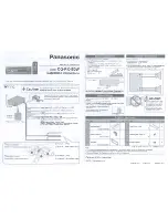
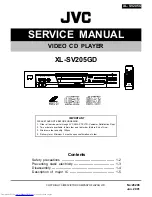
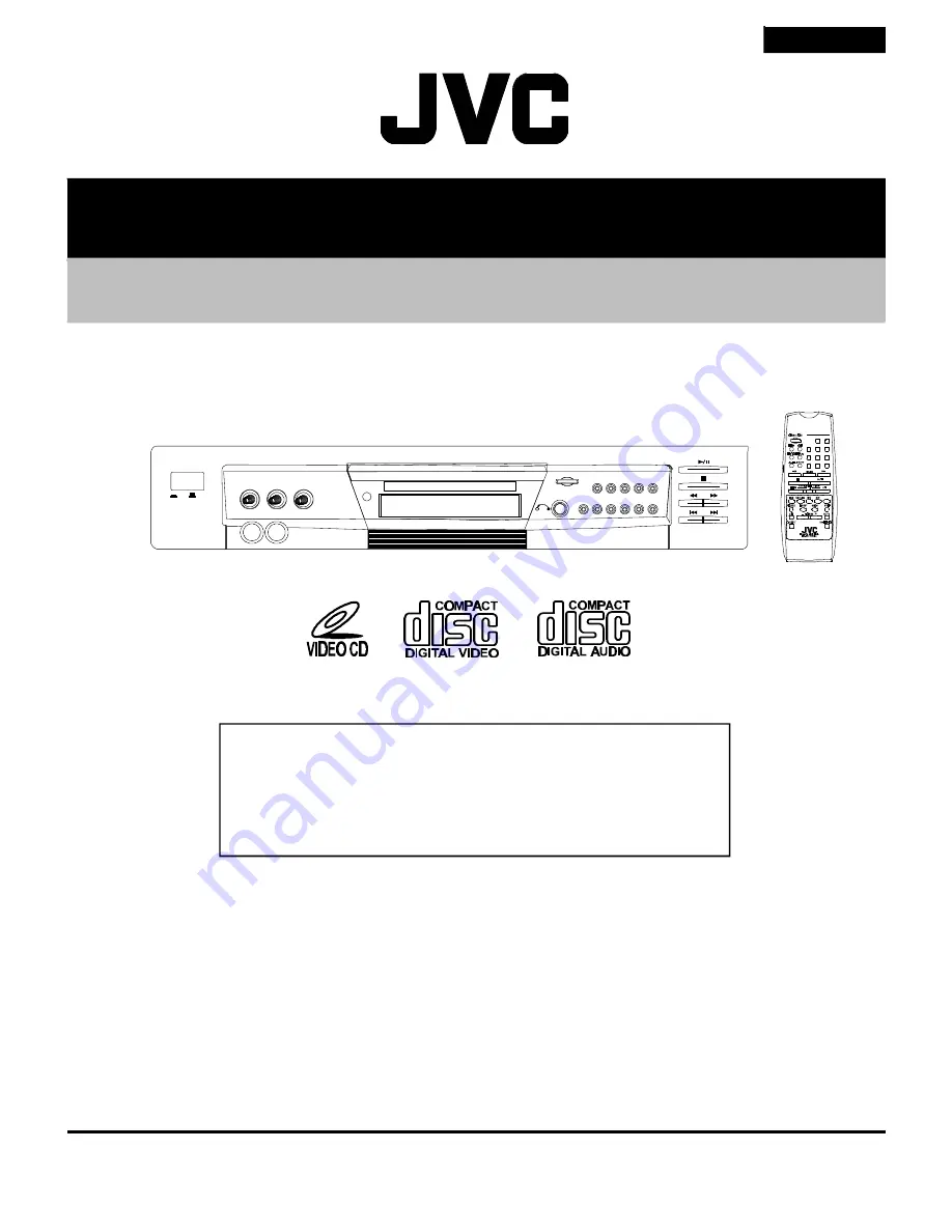
background image

SERVICE MANUAL

VIDEO CD PLAYER

XL-SV205GD

Contents

Safety precautions ------------------------------------------------- 1-2
Preventing static electricity ------------------------------------- 1-3
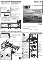
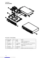
Disassembly ---------------------------------------------------------- 1-4
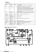
Description of major IC ----------------------------------------- 1-5
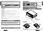
XL-SV205GD

POWER

1 – MIC VOLUME – 2

ECHO

OPEN/CLOSE

RETURN

1 — MIC — 2

1

2

3

4

5

+10

6

7

8

9

10/0

 ON /   OFF

MIN    MAX      MIN     MAX    MIN    MAX

10/0

1

2

3

6

5

4

7

8

9

VCD / CD 10 KEY

10

+

P / N

No:28206
Jun. 2001

COPYRIGHT 

2000 VICTOR COMPANY OF JAPAN LTD.


 IMPORTANT

PLEASE TAKE NOTE BEFORE ORDERING

1.  Order all service parts through JVC ASIA PTE LTD.-Customer Satisfaction Dept.

2.  Two order are availiable: Initial order and last order (Before End of Line).

3.  Minimum order quantity: 100pcs

4.  Delivery term: Minimum 2 months upon confirmation of order.

Summary of Contents for XL-SV205GD

Page 1: ...8 9 10 0 ON OFF MIN MAX MIN MAX MIN MAX 10 0 1 2 3 6 5 4 7 8 9 VCD CD 10 KEY 10 P N No 28206 Jun 2001 COPYRIGHT 2000 VICTOR COMPANY OF JAPAN LTD IMPORTANT PLEASE TAKE NOTE BEFORE ORDERING 1 Order all service parts through JVC ASIA PTE LTD Customer Satisfaction Dept 2 Two order are availiable Initial order and last order Before End of Line 3 Minimum order quantity 100pcs 4 Delivery term Minimum 2 m...

Page 2: ...embling 5 Leakage current check Electrical Shock hazard testing After re assembling the product always perform an isolation check on the exposed metal parts of the product antenna terminals knobs metal cabinet screw heads headphone jack control shafts etc to be sure the product is safe to operate without danger of electrical shock Do not use a line isolation transformer during this check Plug the ...

Page 3: ...uring transport and before installation both sides of the laser diode on the replacement optical pickup are shorted After replacement return the shorted parts to their original condition Refer to the text 2 Do not use a tester to check the condition of the laser diode in the optical pickup The tester s internal power source can easily destroy the laser diode 1 2 Handling the traverse unit optical ...

Page 4: ...ne tray then take up the CD door 3 Self screw 1 Loosen screw Loose the screw remove from the upper cover 4 4 0 Self screw 4 Loosen screw 5 Upper cover 1 Remove Loose screws then remove the upper cover from the main part 6 Self screw 5 Loosen screw 7 Self screw 1 Loosen screw 8 Front panel block 1 Remove Remove the front panel block from the main part ...

Page 5: ...1 5 XL SV205GD IC lead identification internal diagram and description IC301 HT16512 VFD DRIVER Block diagram Pin configuration Top view ...

Page 6: ... outputs data at the falling edge OSC Oscillator pin 44 Connect a resistor to this pin to determine the oscillation frequency to this pin Seg1 KS1 to High voltage 15 to 20 Segment output pins Dual function as key source Seg6 KS6 output Seg7 to seg11 High voltage 21 to 25 Segment output pins output segments Grid1 to Grid6 High voltage 37 to 32 Grid output pins output grid Seg12 Grid11 to High volta...

Page 7: ...1 Current control 1 8 CC0 Current control 0 9 OP1 OUT O OP amplifier 1 output This pin can be used as modulated integrator by connecting capacitor 10 OP1 IN I OP amplifier 1 input This pin can be used as demodulated integrator by connecting capacitor 11 OP2 IN I OP amplifier 2 input This pin can be used as demodulated integrator by connecting capacitor 12 OP2 OUT O OP amplifier 2 output This pin c...

Page 8: ...1 8 XL SV205GD U1 CL680 MPEG 1 DECODER Block diagram Pin configuration IC101 7805 REGULATOR Block diagram ...

Page 9: ... CD LRCK VDDMAX IN CD C2PO VDDMAX IN CDG SCK VDDMAX IN VDDMAX OUT CDG SDATA VDDMAX IN CDG VFSY VDDMAX IN CDG SOS1 VDDMAX IN DRAM Interface MD 15 0 VDDMAX IN VDD3 MA 10 0 VDD3 Signal Input Output RAS 0 VDD3 RAS 1 VDD3 CAS VDD3 MWE VDD3 MCE VDD3 Video Interface PGIO0 VDDMAX IN VDD3 PGIO1 VDDMAX IN VDD3 PGIO2 VDDMAX IN VDD3 PGIO3 VDDMAX IN VDD3 VCK IN VDDMAX IN VREF Analog RREF Analog Y OUT AVDD C OU...

Page 10: ...ess input 14 RAS Input Row address strobe 28 CASH Input Column address strobe Upper byte control 29 CASL Input Column address strobe lower byte control 13 WE Input Write enable 27 OE Input Output enable 2 5 6 10 I O1 I O16 Input Output Data input 31 34 36 39 output 1 6 20 Vcc Supply Power 5V 21 35 40 Vss Ground Ground 11 12 15 30 NC No connect ...

Page 11: ... I A7 A0 5 12 Address input pins I O D0 D2 13 15 Input Output pins GND 16 Ground I O D3 D7 17 21 Input Output pins I CE 22 Chip enable Active low I A10 23 Address input pins I OE 24 Output enable Active low I A11 A9 A8 25 26 27 Address input pins I A13 A14 A17 28 29 30 Address input pins I WE 31 Write enable bar Active low VCC 32 Power supply for device operation 5V 10 U4 CS4338 AUDIO DAC Block di...

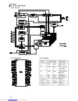
Page 12: ...1 12 XL SV205GD U7 CXD3068Q CD DSP Block diagram Pin description ...

Page 13: ...OR O 1 0 Outputs a high signal when either subcode sync S0 or S1 is detected 16 C4M O 1 0 4 2336MHz output 1 4 frequency division output for V16M in CAV W mode or variable pitch mode 17 WDCK O 1 0 Word clock output f 2Fs GRSCOR is output by the command switching 18 DVss0 Digital GND 19 COUT I O 1 0 Track count signal I O 20 MIRR I O 1 0 Mirror signal I O 21 DFCT I O 1 0 Detect signal I O 22 FOK I ...

Page 14: ... wide band EFM PLL clock input by switching with the command 60 VPCO O 1 Z 0 Wide band EFM PLL change pump output 61 DVDD2 Digital power supply 62 ASYE I Asymmetry circuit on off low off high on 63 MD2 I Digital Out on off control low off high on 64 DOUT O 1 0 Digital Out output 65 LRCK O 1 0 D A interface LR clock output f Fs 66 PCMD O 1 0 D A interface Serial data output two s complement MSB fir...

Page 15: ...onnect to GND for 1 75 power supply connect a smoothing capacitor for single 3 5V Power supply 11 TE O Tracking error amplifier output pin E F signal is output 12 FE_BIAS I Bias adjustment pin for inverted side of focus error amplifier 13 FE O Focus error amplifier output pin 14 FRM I RF amplifier inverted side input pin RF amplifier gain is determined by the resistor connected between this pin an...

Page 16: ... power block 11 VO2 Inverted output of CH2 12 VO2 Non inverted output of CH2 13 VO1 Inverted output of CH1 14 VO1 Non inverted output of CH1 15 VO4 Non inverted output of CH4 16 VO4 Inverted output of CH4 17 VO3 Non inverted output of CH3 18 VO3 Inverted output of CH3 19 PowVcc2 Vcc for CH3 4 power block 20 STBY2 Input for CH4 stand by control 21 GND Substrate ground 22 OPOUT3 Output for CH3 OP AM...

Page 17: ...JVC Asia Pte Ltd 101 Thomson Road 28 04 United Squares Singapore 307591 No 28206 Printed in Japan XL SV205GD 200102 L ...

Page 18: ...E LTD Customer Satisfaction Dept 2 Two order are availiable Initial order and last order Before End of Line 3 Minimum order quantity 100pcs 4 Delivery term Minimum 2 months upon confirmation of order Contents Exploded view diagram 3 2 Mechanical parts list 3 3 Electrical parts list 3 4 Packing list 3 8 Parts ordering form 3 9 ...

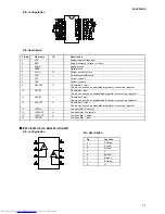
Page 19: ...3 2 XL SV205GD Exploded view diagram Main unit exploded view diagram ...

Page 20: ... S TAP SCREW P B 4X6 8 14 459 SV2001 01 HOLDERMECH 1 1 15 E4103 020001 SWITCH SLIDE LZ1 22A2 4410206199 1 16 459 SV2002 01 HOLDERMECH 2 1 17 E7701 005001 MECHANISM VCD KSS 213V 1 18 211 SV2001 02S PANEL TRAY W SILK SV20 S 1 19 402 SV2001 01 PANEL REAR 1 20 E7801 006001 PCB ASSY HY 24AVER1 6 1 21 322 SV2002 01Y CUSHION FOOT BACK 2 22 403 SV2001 01 CHASSIS BOTTOM 1 23 610 260108 00 S TAP SCREW RND 2...

Page 21: ...C128 E1301 041012 CAPACITOR EC V SAII 102M 16DC 1 C127 E1301 041013 CAPACITOR EC V SAII 222M 16DC 1 C108 E1301 041025 CAPACITOR EC V A SAII 332M 16DC 13X25 1 C104 E1321 002002 CAPACITOR CE V HIK F 103Z 50DC T05 8 8 C105 E1321 002002 CAPACITOR CE V HIK F 103Z 50DC T05 8 8 C106 E1321 002002 CAPACITOR CE V HIK F 103Z 50DC T05 8 8 C107 E1321 002002 CAPACITOR CE V HIK F 103Z 50DC T05 8 8 C123 E1321 002...

Page 22: ...IRE WD CG 2N 0140 D0A D0A 1 B1 B2 E3451 000079 WIRE WD CG 3N 0140 D0A D0A 1 C1 C2 E3451 000215 WIRE WD CG 4N 0140 DOA DOA 1 E3701 00L010A PCB POWER SUPPLY 168X68 V0 1 E3701 00L010B PCB AC SELEC V0 1 E3701 00L010C PCB AC SW V0 1 SW102 E4101 023001 SWITCH POW KDC A09 1 SW101 E4103 020001 SWITCH SLIDE LZ1 22A2 4410206199 1 L101 E4405 021001 FILTER LINE LCL 2002WH 1 Electrical parts list Power board R...

Page 23: ...1 001033 RESISTOR CBF H 1 6W 223J T52 2 R216 E1501 001033 RESISTOR CBF H 1 6W 223J T52 2 R202 E1501 001050 RESISTOR CBF H 1 6W 303J T52 2 R212 E1501 001050 RESISTOR CBF H 1 6W 303J T52 2 R221 E1501 001067 RESISTOR CBF H 1 6W 472J T52 3 R233 E1501 001067 RESISTOR CBF H 1 6W 472J T52 3 R234 E1501 001067 RESISTOR CBF H 1 6W 472J T52 3 R230 E1501 001068 RESISTOR CBF H 1 6W 473J T52 1 R232 E1501 001076...

Page 24: ...C301 E2351 077001 IC HT16512 1 D301 E2501 010001 DIODE SILICON H 1N4148 T72 T52 5 D302 E2501 010001 DIODE SILICON H 1N4148 T72 T52 5 D303 E2501 010001 DIODE SILICON H 1N4148 T72 T52 5 D304 E2501 010001 DIODE SILICON H 1N4148 T72 T52 5 D305 E2501 010001 DIODE SILICON H 1N4148 T72 T52 5 OP301 E2701 017002 DETECTOR IR SPS 440 1 E 1 JP301 JP325 E3409 001001 WIREJUMPER0 6MM1KG 375M 0 0005 JP326 E3409 0...

Page 25: ... XL SV205GD Main Part 1 5 310 222406 04V Polybag 1 6 580 SV2001 025 INST Booklet E C A 1 7 310 101504 02T Polybag 1 8 510 SV2001 01A Gift Box 1 9 300 SV2002 01C Polyfoam R 1 10 310 051004 03V Polybag 2 11 E3402 008001 AV Line 1 12 579 SV2001 03 Bar Code Label 1 13 E3103 003001 Conversion Flat to Round UX 1 14 E3103 004001 Conversion Round to Flat U 1 ...

Page 26: ...nature Chop Destination Ship Via AIR AIR MAIL DHL MAIL SEA SEA MAIL SEA AIR Account Code Destination Code Purchase Order No Item No Model No Parts No Parts Name Qty Remarks Please do not forget to describe Model No with Tail code 3 9 ASIA PTE LTD PAGE ______OF_____ PARTS ORDERING FORM ...

Page 27: ... 0 ON OFF MIN MAX MIN MAX MIN MAX 10 0 1 2 3 6 5 4 7 8 9 VCD CD 10 KEY 10 P N No 28206sch Jun 2001 COPYRIGHT 2000 VICTOR COMPANY OF JAPAN LTD IMPORTANT PLEASE TAKE NOTE BEFORE ORDERING 1 Order all service parts through JVC ASIA PTE LTD Customer Satisfaction Dept 2 Two order are availiable Initial order and last order Before End of Line 3 Minimum order quantity 100pcs 4 Delivery term Minimum 2 mont...

Page 28: ...2 1 XL SV205GD Wiring diagram ...

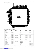
Page 29: ...2 2 XL SV205GD Block diagram ...

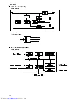
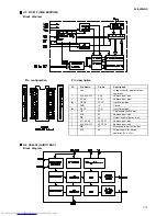
Page 30: ...XL SV205GD 2 3 Schematic Diagrams MIC AMP Power Key FLD Circuit ...

Page 31: ...37 IO15 38 IO16 39 VSS3 40 U2 814260 D1 D2 D3 D4 D5 D6 D7 D8 D9 D10 D11 D12 D13 D14 D15 D0 A0 A1 A2 A3 A4 A5 A6 A7 A8 A9 A10 A0 A1 A2 A3 A4 A5 A6 A7 A0 A1 A2 A3 A4 A5 A6 A7 A8 A8 A9 A10 D0 D1 D2 D3 D4 D5 D6 D7 D8 D9 D10 D11 D12 D13 D14 D0 D1 D2 D3 D4 D5 D6 D7 D8 D9 D10 D11 D12 D13 D14 D15 C116 104 5VM 5VM R116 1K R114 2K C111 104 C112 47U C113 47U C114 104 C115 104 L4 XUH R115 2 2K 3V3 DAC C106 10...

Page 32: ...FE_BIAS 12 FE 13 RFM 14 RFO 15 RF1 16 RFTC 17 AGCCOUT 18 LD_ON 19 VCC 20 U8 CXA2550 C77 102 C80 104 C79 104 C81 104 C40 104 C88 224 C52 104 C59 104 C51 471 C49 103 C50 474 C61 474 C60 104 C62 101 C63 470P C47 104 C46 471 C54 104 R86 OPEN C57 10U R85 OPEN R55 4E7 R65 10E R66 120K R71 120K R44 33K R45 10K R46 100K R47 10K R51 470K R50 1M R52 820K R49 180K R48 1K R41 10K R40 15K Q11 BC328 40 Q12 BC32...

Page 33: ...04 C25 104 C31 104 C30 47U A R0 A R1 A L0 A L1 RST 680 VIDEO MIC MUTE 1 2 3 4 5 6 7 8 9 JP7 A V C29 104 RF V 9 8 U10D 74U04 D1 1N4148 AUD5V AOUTR AOUTL C11 10U 50V 1 2 3 4 JP8 4PIN Z1 5 1V 12V R16 10K 5VM DA LRCK DA DATA DA BCK 16M9 SDATA 1 SCLK 2 LRCK 3 MCLK 4 AOUTR 5 AGND 6 VA 7 AOUTL 8 U4 4338 1 2 3 4 5 6 7 8 9 10 JP1 10PIN C1 100U 16V C2 100U 16V C3 100U 16 C4 47U 16V C5 47U 16V C6 104 C7 104 ...

Page 34: ...XL SV205GD 2 7 Printed Circuit Boards Power supply AC selector AC switch board Top view ...

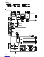
Page 35: ...XL SV205GD 2 8 MPEG Servo Output Board Fig 1 ...

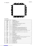
Page 36: ...XL SV205GD 2 9 MPEG Servo Output Board Fig 2 Fig 3 ...

Page 37: ...JVC Asia Pte Ltd 101 Thomson Road 28 04 United Squares Singapore 307591 No 28206 Printed in Japan XL SV205GD 200102 L ...

Reviews: