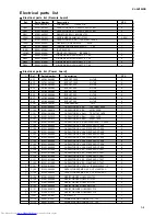


XL-SV205GD
2-5
§
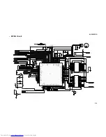
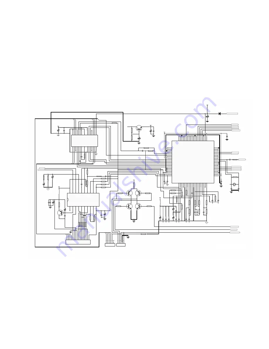
Servo Circuit
OUT1+
1
OUT1-
2
OUT1
3
IN1-
4
IN1+
5
VREFIN
6
VCC/2
7
GND0
8
IN2+
9
IN2-
10
OUT2
11
OUT2+
12
OUT2-
13
GND1
14
MUTE
15
OUT3+
16
OUT3-
17
OUT3
18
IN3-
19
IN3+
20
VCC0
21
VCC1
22
IN4+
23
IN4-
24
OUT4
25
OUT4+
26
OUT4-
27
GND2
28
GND3
29
GND4
30
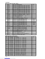
U9
BA6392AFP
DVDD0
1
XRST
2
MUTE
3
DATA
4
XLAT
5
CLOK
6
SENS
7
SCLK
8
ATSK
9
WFCK
10
XUGF
11
XPCK
12
GFS
13
C2PO
14
SCOR
15
C4M
16
WDCK
17
DVSS0
18
COUT
19
MIRR
20
DFCT
21
FOK
22
PWMI
23
LOCK
24
MDP
25
SSTP
26
FSTO
27
DVDD1
28
SFDR
29
SRDR
30
TFDR
31
TRDR
32
FFDR
33
FRDR
34
DVSS1
35
TEST
36
TES1
37
VC
38
FE
39
SE
40
TE
41
CE
42
RFDC
43
ADIO
44
AVSS0
45
IGEN
46
AVDD0
47
ASYO
48
ASYI
49
RFAC
50
AVSS1
51
CLTV
52
FILO
53
FILI
54
PCO
55
AVDD1
56
BIAS
57
VCTL
58
V16M
59
VPCO
60
ASYE
62
DVDD2
61
MD2
63
DOUT
64
LRCK
65
PCMD
66
BCK
67
EMPH
68
XTSL
69
DVSS2
70
XTAI
71
XTAO
72
SOUT
73
SOCK
74
XOLT
75
SQSO
76
SQCK
77
SCSY
78
SBSO
79
EXCK
80
U7
CXD3068Q
C68
220U
C72
1U
D10
D4148
C73
100U
C78
100U
C76
100U
C82
10U
C58
100U
C53
100U
VDD
C69
104
C70
334
C71
104
C41
10u/16v
C74
103
R88
10k
C75
47P
C42
683
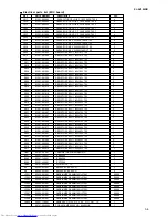
AGCVTH
1
LD
2
PD
3
PD1
4
PD2
5
VEE
6
F
7
E
8
EI
9
VC
10
TE
11
FE_BIAS
12
FE
13
RFM
14
RFO
15
RF1
16
RFTC
17
AGCCOUT
18
LD_ON
19
VCC
20
U8
CXA2550
C77
102
C80
104
C79
104
C81
104
C40
104
C88
224
C52
104
C59
104
C51
471
C49
103
C50
474
C61
474
C60
104
C62
101
C63
470P
C47
104
C46
471
C54
104
R86
OPEN
C57
10U
R85
OPEN
R55
4E7
R65
10E
R66
120K
R71
120K
R44
33K
R45
10K
R46
100K
R47
10K
R51
470K
R50
1M
R52
820K
R49
180K
R48
1K
R41
10K
R40
15K
Q11
BC328-40
Q12
BC328-40
Q9
BC338-40
Q8
BC338-40
Q10
8550
R77
4E7
R75
680E
R76
680E
R64 100K
R63 15K
R62 15K
R61 10K
R60
150
R84
0E
R58
2K
R83
OPEN
R54
150K
R82
OPEN
L7
XUH
R81
3K3
1
2
3
4
5
6
7
8
9
10
11
12
13
14
15
16
JP2
CON16
R80
1K8
1
2
3
4
5
6
JP3
CON6
R79 10K
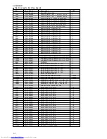
F-
T-
T+
F+
PD
LD
F
C
B
A
D
E
VC
L8
XUH
VDD
R57
1K
R56
1M
SONY 3068 SCHEMATIC
T-
T+
F-
F+
AGC
LDON
C48
152
C55
104
C56
104
C64
104
VDD
SL+
SL-
SP+
SP-
SP-
SP+
SL+
SL-
VDD
VC
+5VM
+5VS
CLOSE
OPEN
TRAY-SW
C44
47U/16V
R42
1K
R43
270
Q7
8050
+8V
R59
3K
VC
R70
56K
R69
56K
R68
56K
R67
56K
VDD
SENS
CLOK
XLAT
2DATA
RST-3068
SCOR
CD-DATA
CD-LRCK
CD-BCK
SQSO
SQCK
VDD
R72
10K
SE
TE
FE
VC
RF
R74
1K2
FRDR
R73
1K2
FRDR
FFDR
FFDR
TRDR
TRAY-
TRDR
TRAY+
TFDR
TFDR
SRDR
TRAY-SW
SRDR
OPEN
SFDR
CLOSE
SFDR
SQSO
MDP
SQCK
MDP
2DATA
XLAT
CLOK
X2
16M9
SENS
R78
6K8
SCOR
R53
100E
AGC
C65
20P
LDON
C66
20P
MDP
C67
102
16M9
SW
C43
220U
C45
104
SE
TE
FE
RF
VC
CL
OP
VR
VEE
AVDD0
CLTV
RFTC
VCC
1
2
3
4
5
JP4
CON5
SW
SW
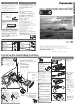
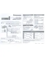
Summary of Contents for XL-SV205GD
Page 12: ...1 12 XL SV205GD U7 CXD3068Q CD DSP Block diagram Pin description ...
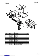
Page 19: ...3 2 XL SV205GD Exploded view diagram Main unit exploded view diagram ...
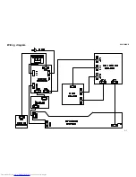
Page 28: ...2 1 XL SV205GD Wiring diagram ...
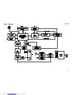
Page 29: ...2 2 XL SV205GD Block diagram ...
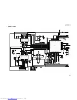
Page 30: ...XL SV205GD 2 3 Schematic Diagrams MIC AMP Power Key FLD Circuit ...
Page 34: ...XL SV205GD 2 7 Printed Circuit Boards Power supply AC selector AC switch board Top view ...
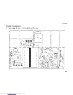
Page 35: ...XL SV205GD 2 8 MPEG Servo Output Board Fig 1 ...
Page 36: ...XL SV205GD 2 9 MPEG Servo Output Board Fig 2 Fig 3 ...