Komodo Frame Grabber User Guide
20
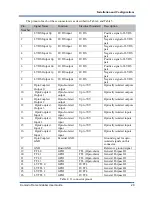
The pinout of each of these connectors is as described in Table 4 and Table 5.
Pin
Number
Signal Name
Function
Electrical Standard
Description
1
LVDS Input 0p
LVDS input
LVDS
Positive signal of LVDS
pair
2
LVDS Input 0n
LVDS input
LVDS
Negative signal of LVDS
pair
3
LVDS Input 1p
LVDS input
LVDS
Negative signal of LVDS
pair
4
LVDS Input 1n
LVDS input
LVDS
Negative signal of LVDS
pair
5
LVDS Output 0p
LVDS output
LVDS
Positive signal of LVDS
pair
6
LVDS Output 0n
LVDS output
LVDS
Positive signal of LVDS
pair
7
LVDS Output 1p
LVDS output
LVDS
Negative signal of LVDS
pair
8
LVDS Output 1n
LVDS output
LVDS
Negative signal of LVDS
pair
9
OptoCoupled
Output 0
Opto-Isolated
output
Up to 70V
Optically isolated outputs
10
OptoCoupled
Output 1
Opto-Isolated
output
Up to 70V
Optically isolated outputs
11
OptoCoupled
Output 2
Opto-Isolated
output
Up to 70V
Optically isolated outputs
12
OptoCoupled
Output 3
Opto-Isolated
output
Up to 70V
Optically isolated outputs
13
OptoCoupled
Input 0
Opto-Isolated
input
Up to 70V
Optically isolated inputs
14
OptoCoupled
Input 1
Opto-Isolated
input
Up to 70V
Optically isolated inputs
15
OptoCoupled
Input 2
Opto-Isolated
input
Up to 70V
Optically isolated inputs
16
OptoCoupled
Input 3
Opto-Isolated
input
Up to 70V
Optically isolated inputs
17
OptoCoupled
GND
External GND
Ground signal for opto-
isolated signals on this
connector.
18
GND
Board GND
Reference ground signal
19
TTL 0
GPIO
TTL (Open-drain)
General Purpose IO
20
TTL 1
GPIO
TTL (Open-drain)
General Purpose IO
21
TTL 2
GPIO
TTL (Open-drain)
General Purpose IO
22
TTL 3
GPIO
TTL (Open-drain)
General Purpose IO
23
LVTTL 0
GPIO
LVTTL
General Purpose IO
24
LVTTL 1
GPIO
LVTTL
General Purpose IO
25
LVTTL 2
GPIO
LVTTL
General Purpose IO
26
LVTTL 3
GPIO
LVTTL
General Purpose IO
Table 4: J1 connector pinout
Installation and Configurations


