background image

Check out and Calibration:

C

lean the board of any flux residue. This will help in inspecting all the solder connections. “Electrical Parts Cleaner”, 

available at most commercial electrical parts suppliers works well to remove flux. Denatured alcohol will also work. Avoid 
rubbing  alcohol, as this leaves a white residue.  Using your magnifier, inspect all the solder connections, looking in 

particular for any you might have missed making. Hopefully, you have all the ICs installed with the proper orientation and 
location, as this type of error is not easy to correct. Same goes with the caps, as it’s now difficult to verify their correct 

values. 

If you have already installed L14, remove it before doing the initial power up tests. 

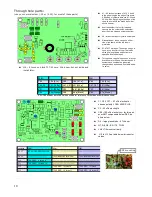
Use an ohm meter to check for shorts across the DC in, +3.5 and +5 regulator outputs to ground. 

Find and eliminate short if one is detected. 

Wire up a 9V supply to the power plug (Use 9V battery or current limited supply set to 50 ma limiting) to start. This 
way, if there is a problem, its unlikely any damage will result from too much current being drawn. 

 Plug a set of stereo headphones into the headphone jack. 

Plug in the power supply

You should hear the power up message “4” or “2” in the headphones and see a that number appear on the LED display. 
If you hear this message, you know the processor and audio amp are working fine. 

Check the voltage at TP1, it should be 0 volts. If not, check connections on R19.

Check the voltage on the PA gates, Q7 to Q9. This voltage should be zero (0) volts. If it is not, check solder 
connections on U8 pins. 

Plug a paddle into the paddle jack and send some dits and dahs. You should of course, hear them in the headphones. 

Connect a voltmeter between ground and the Drain of Q5, the PA keying transistor. (Large metal tab is Drain). 

Send a string of Dahs and watch the voltmeter. The voltage reading should go to near the DC supply input voltage. It 
should then slowly decay to zero when you stop sending. This is the voltmeter discharging the .1 uF bypass cap. Check 

the soldering in the keying circuit if there is a problem.  

Remove power from the board. 

You can now install L14.   

Reference Oscillator Frequency Calibration:

NOTE: Entering the calibration mode will rest the reference, offset and initial power on frequencies to their default values. 

This is done to ensure “known good values” are used in the off chance the stored values become corrupted. 

The “ideal” reference frequency of 40.000,000 MHz is initially assumed to calculate the DDS  VFO frequency. In practice, 
the reference oscillator has a +/- 100 ppm tolerance. This tolerance can cause an error between what the processor thinks 

the operating frequency is and what it really is. The error would be most noticeable on the higher bands, where the 
reference clock is less divided.  Therefore, this calibration is provided to adjust the value of the reference frequency value 

used in the DDS frequency calculation to exactly match the actual oscillator frequency and therefore produce the expected 
operating frequency. 

However, the typical error is small enough that if you don't have an accurate frequency counter, it is usually best to use the 

default values and “click past” this part of the calibration. 

This calibration is most easily done with an accurate frequency counter. If you do not have access to one, but do have a rig 
with general coverage, good calibration and can tune to 10 MHz, then you can use that. If you can connect up a PSK 

program or other audio spectrum analyzer software which can show you the audio frequency of the signal from the rig's 
audio, this will help a lot. Set the rig to receive USB at 9.999,000 MHz. This will cause a 1 kHz beat note when a 

10.000,000 MHz signal is received. The PSK waterfall can be used to show you when you have adjusted the DDS frequency 
to produce the exact 1 kHz beat note. A short pick up wire attached to a piece of coax going to the rigs antenna jack and 

placed near the TP1 test point should pick up plenty of signal. If you have no means of accurately measuring 10 MHz, skip 
through this procedure by clicking the 

MENU

 switch after step 6 and go directly to the LO cal procedure. 

 
1. Click and hold closed both the 

RIT

 and 

Tune UP

 switches. 

2. Apply power.

3. “CR” will be annunciated by the side tone. “C” and then “r” will appear on the LED display when calibration mode is 

enabled. 

4. Release the switches. 

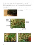
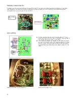
5. Connect a frequency counter to DDS TP1.
6. Wait a minute or two for the oscillator to stabilize. 

7. Using the tune up and tune down switches, adjust the frequency at TP1 to exactly 10.000,000 MHz. 
8. Once the frequency is adjusted, click the MENU switch to store the new reference frequency. 

9. The side tone will now announce “CO” A low pitched tone will be heard in the headphones. The display will change to 

“o”

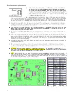
NOTE: if you don't get any output from the DDS, often times this is due to a bad or missing solder connection to one of the 

12

Summary of Contents for Mountain Topper

Page 1: ...ncy trim and BFO adjustment 13 Receiver input peaking 13 Transmitter test and output low pass filter adjustment 13 Mounting into an enclosure 16 Basic operation 17 Turning the rig on and off 17 Volume control 17 Band selection 17 Control switches 17 Frequency tuning 18 Tuning limits 18 SPLIT MODES 18 MENU 18 Quick selections 18 DFE Mode 19 Tune Mode 19 Battery Voltage 19 MENU switch only selected ...

Page 2: ...ing heat to the end of the part over the tined circuit board pad while applying a little pressure to make sure it lays flat to the board Be sure to heat both the pad and the end of the part Generally you will not have to add any additional solder to this connection Then solder the other end of the part If you don t do this right away and go onto tacking down some more parts there is a good chance ...

Page 3: ...e also color coded but with a color sticker as they come in plastic carriers Again the color on the carrier matches the color shown on the placement guide diagram Resistors have their value printed on them though it might take a magnifying glass to read the numbers Therefore individual values are not color coded Various photos Using a straight edge to hold the TSSOP IC s in alignment with the pads...

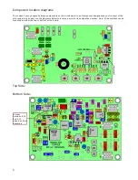
Page 4: ...d to put component designations next to most of the chip resistors and caps Use the diagrams below to locate a part with its designation number Note Slide switches can be mounted on either the top or bottom of the board Top Side Bottom Side 4 Jumper between R14 and R13 added on final assembly ...

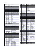
Page 5: ... L1 L2 L9 SMT 1206 2 18 uH 40M BRN GRY BLK GLD 2 12 uH 30M BRN RED BLK GLD 2 8 2 uH 20M GRY RED GLD GLD QTY Part number Color code or value location description 2 SA612A U1 U3 MIXER 1 LM4808M U2 AUDIO AMP 1 TC1014 3 3VCT713 BROWN A5xx last two characters are date code U4 3 3V REG 1 LM386M U5 AUDIO AMP 1 AD9834BRUZ U6 DDS 1 MCP1703 5002E DB MCP1703 U7 5V REG 1 74AC02M AC02 U8 QUAD OR 1 SN74LVC1G315...

Page 6: ...ut diagram U11 is the rectangular box with the silver top Be sure to get solder to flow into the little U shaped cups near each corner of the part A number of builders have had trouble with this and not made solder connection to the pads under the part A fine tipped iron is required here Also be careful of using too much solder and making a short to the metal top of the package D3 has very faint l...

Page 7: ...rs left over which go on the top side of the board Put these aside in a safe place until needed The approximate location in the table will help locate the position of the resistor values on the board upper middle lower is Y coordinates area while left center right is X coordinates Resistors R3 BS1 and R4 BS2 values depend on the band to be used see band value table below 7 Value places Approximate...

Page 8: ... a safe place for the time being light blue red stripe 1 Brown 1 Orange 1 Red 3 Blue 2 It is easy to confuse the orange caps 22 pfd with the Red 0 1 ufd caps on the layout digram so we will pace the orange ones first Part number start in upper left and run left to right top to bottom in a zig zag fashion 8 Location color places C18 30 32 68 Orange 4 C25 26 Yellow green stripe 2 C4 5 6 8 9 11 21 22...

Page 9: ...t confuse with Q6 2955 Q6 7 seg display LED Display Make sure decimal point is in lower right hand corner Once soldered in place the display is nearly impossible to remove Four trimmer capacitors labeled BNDB and BNDA now need to be installed before the through hole parts are mounted to the top side of the board CT1 is on the bottom side Install this one now Note the cut corners on one end of the ...

Page 10: ...hole caps Values shown in layout locations are for 40 and 20 meter bands If another band combination is desired change values as needed See table below for value 20M 40M 30M C60 104 0 1u C60 104 0 1u C60 104 0 1u C46 56 151 150 p C47 C57 331 330 p C47 C57 221 220p C51 331 330 p C52 681 680 p C52 561 560p C65 22p Orange C66 68 p Black C66 47p Brown C65 C66 already installed values shown for referen...

Page 11: ...ing Cut the insulated hookup wire to lengths about 1 5 long Install the wires to the top side of the board then connect to the corresponding connections on the jacks If mounting the board in an Altoids tin the jacks will mount as close to the bottom side of the board as possible In order for this to work the wires need to come off the top side of the board and wrap back around the edge to connect ...

Page 12: ...the off chance the stored values become corrupted The ideal reference frequency of 40 000 000 MHz is initially assumed to calculate the DDS VFO frequency In practice the reference oscillator has a 100 ppm tolerance This tolerance can cause an error between what the processor thinks the operating frequency is and what it really is The error would be most noticeable on the higher bands where the ref...

Page 13: ...transmitter and filter boards are working properly You can now go onto the testing and adjusting the band filters Otherwise go to the trouble shooting guide on page and track the reason the rig isn t working down Receiver input peaking The two trimmers labeled BNDB peak the band selected with the slide switches set to the right normally 20 Meters Like wise the two trimmers labeled BNDA peak the ba...

Page 14: ...de drop Output from 5V and 3 3 V regulators If not check connections and for shorts to ground Connections to U10 the processor Check power supply pins and X6 crystal connections The processor will not do anything except set the ports direction and state unless the 32 kHz clock is running Missing segments on LED display Check connections on R31 to R38 on the display and processor leads No receive C...

Page 15: ...V Tx key P6 1 7V osc P23 3 3V Tune up P7 3 3V reset P22 3 3V MENU P8 3 3V Tune dn P21 3 3V RIT P9 3 3V Dash in P20 0 3 3V Band volt P10 3 3V Dot in P19 5 to 1 2 Batt V P11 3 3V 7seg P18 3 3V 7seg P12 3 3V 7seg P17 3 3V 7seg P13 3 3V 7seg P16 3 3V 7seg P14 3 3V 7seg P15 3 3V 7seg U10 MPS430 MPU P1 1 13V FS ADJ P20 75V IOUTB P2 1 17V REF out P19 37V IOUT P3 1 76V COMP P18 0V AGND P4 3 3V AVDD P17 37...

Page 16: ...ill locate the holes for the jacks Drilling the thin sheet metal of the tin does not generally result in the cleanest holes The best results are obtained if you have a drill press You should always make a dimple to center to drill bit with a center punch or other shape pointy object Then drill a pilot hole using a small diameter bit say 1 16 This will keep the larger bits from wandering when you m...

Page 17: ...tually produce too much volume if your hearing is still good In this case an in line volume control can be added in series with your headphones Band selection Three DPDT switches are used to select one of the two bands the rig has been built for Make sure all three switches are in the same position i e to the right or to the left The switch near the top edge of the case tells the processor which b...

Page 18: ... RIT mode While RIT is active the display is used to show the approximate Rx frequency delta relative to the Tx frequency as illustrated by the diagram A 0 is displayed when Rx Tx frequency A side tone beep is also sounded when you tune back to the frequencies being equal When you tune above or below the Tx frequency but by less then 250 Hz the display will show When you tune beyond delta 250 Hz L...

Page 19: ...t carrier is not needed it is better to send a string of Dots then use Tune mode for adjusting a tuner Toggle transmitter on Tap the LEFT DOT paddle Toggle transmitter off Tap RIGHT DASH paddle Exit Tune mode Click Menu switch E annunciated Battery Voltage This mode reads the input voltage to the board and then displays it on the LED display and annunciated in Morse The letter B is sent before the...

Page 20: ...al and the upper right segment b will flash at the word space time out Paying attention to the flashing lights will allow you to enter a message without timing mistakes Checking and storing the message When you have finished keying in the messages click the Menu switch The message will then play back so you can check that they were entered correctly If the playback is good and there are no mistake...

Page 21: ...can be restored using the calibration mode which will also reset the initial power on frequencies Straight key mode Straight key mode is automatically detected and enabled when the rig is powered up when a monaural plug is in the paddle jack The sleeve of the mono plug grounds the dash input which enables straight key mode Straight key mode also allows use of an external keyer if one so desires Op...

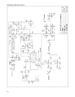
Page 22: ...Schematics Receiver section 22 ...

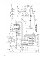
Page 23: ...CPU TRANSMITTER Sections 23 ...

Page 24: ...un it Of course you do click yes A comprehensive operations manual for Pocketdigi has yet to be written Vojtech in waiting for someone to volunteer Most of the functions are self evident and intuitive working in much the same way as programs you are probably familiar with The screen is divided into three sections The top is the waterfall The operating frequency is set by tapping or clicking on the...

Page 25: ...n tones and can be heard in the headphones 4 Find the ATS 3B signal with the other receiver and select the signal on the waterfall Its AFC should also be turned off 5 Return to receive mode on the Pocketdigi by clicking the lightning bolt again 6 Transmit a signal with the other rig 7 Check the frequency of where the other rig is transmitting at on the Pocketdigi water fall Tune the transmit frequ...

Page 26: ... Notes taken from QSO data soft Software version Making QSOs Because the bandwidth of the MTR is so narrow you have to tune stations in to get them into the pass band Once in the pass band of the receiver and you have good copy on them you can match their frequency by taping on the waterfall This is very handy as the 50 Hz tuning steps are a little too coarse to exactly match other stations freque...

Reviews: