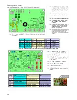
Semiconductor placement
●
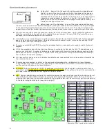
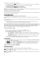
Finding Pin 1. Some of the ICs used in this kit have a dot or indentation at
the Pin 1 corner of the chip. For others, the Pin 1 locations isn't as obvious.
The manufactures logo is sometimes used (as is the case for U1 and U3) or
sometimes there is a line along the Pin 1 end of the chip. In all cases, there is
a beveled or rounded edge along the side of the Pin 1 (left) side of the IC
package. When the chip is viewed so the package is orientated vertically, Pin 1
is always in the upper left corner.
●
Before placing an IC or transistor, tin one of the corner pads and then tack
that lead of the part down first. Before soldering any other pins, make sure all the leads are lined up on the pads.
This is especially important for U6 and U10, where these isn't much room for error. Then solder the lead on the
opposite corner from the tacked lead to make sure the body doesn't move when you solder the rest of the leads.
●
You will have to carefully check the number on the 8 pins IC's to tell them apart. Using a magnifying glass and
tilting the part slightly to the light will aid in reading the a part number. The rest of the IC's are each in unique
packages, so are easier to determine their locations.
●
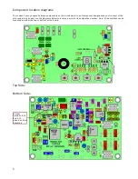
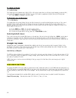
U4 and U9 are very similar. The way to tell them apart is the fact U4 has 5 leads and U9 has 6. To help tell them
apart, U4 has been color coded Brown. U9 has a faint dot which marks the pin 1 end, also the lettering “CC5R”
will be upside down when installed correctly.
●
There are several different SOT-23 devices, the packages they are in are each color coded to match the layout
diagram.
●
U11 is the rectangular box with the silver top. Be sure to get solder to flow into the little “U” shaped cups near
each corner of the part. A number of builders have had trouble with this and not made solder connection to the
pads under the part. A fine tipped iron is required here. Also, be careful of using too much solder and making a
short to the metal top of the package.
●
D3 has very faint line on one end to indicate the cathode end. Look carefully for this line and face it towards the
line printed on the board.
●
There maybe more numbers or letters on the semiconductor packages then indicated on the layout diagram.
These are date or lot codes and can vary depending on when the parts are purchased. Therefore these are not
used for part identification on the layout diagrams.
●
CAUTION! There are three parts in SOT-223 packages, one of which is the 5V regulator, which goes on the top
side of the board.
Do not mix up with the 2955 MOSFETS, Q5 and Q6
. The regulator is loose in the semiconductor
parts bag, while the two MOSFETS are together in a parts carrier.
●
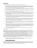
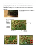
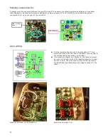
HINT: Taping a straight edge, such as a thin metal ruler, across the board and lined up with the bottom outline of
U6 or U10 (as the case maybe) will aid in keeping the part aligned with the pads. First do U6, then U10. After
soldering the leads, clean up any solder shorts with the supplied solder wick. Be sure to only pull the wick parallel
to the leads, not against the gain! (see picture, page 3)
6
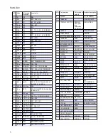
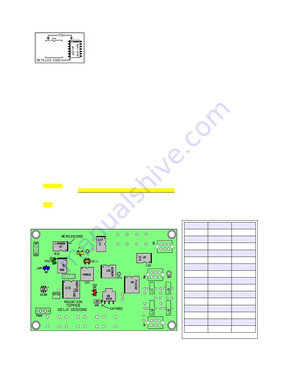
LOCATION
PART #
PACKAGE
U6
AD9834
TSSOP-20
U10
F2132
TSSOP-28
Q1
Green/G1U
SOT-23
Q2
Blue/ 1AM
SOT-23
Q4
Red/702
SOT-23
D1
Yellow /A7
SOT-23
U1/U3
SA612A
SO-8
U2
LM4808
S0-8
U5
386
S0-8
U8
74AC02
SO-14
D3
-- W8
2 leads
U4
Brown/A5xx SOT23-5
U9
---- CC5R
SOT-23-6
U11
40.00
silver
Q5
2955
SOT-223
Remember, Q5 is in parts carrier, not loose
Summary of Contents for Mountain Topper
Page 22: ...Schematics Receiver section 22 ...
Page 23: ...CPU TRANSMITTER Sections 23 ...


