background image

Summary of Contents for AUTO-PROBE 167

Page 1: ...INSTRUCTION MANUAL MODEL 167 AUTO PROBE DIGITAL MULTIMETER ICEITHLEY irsrSTRU VnEIS TS...

Page 2: ...ill be given assist ance and shipping instructions REPAIRS AND RECALIBRATION Keithley Instruments maintains a complete re pair service and standards laboratory in Cleve land and hasan authorized field...

Page 3: ...INSTRUCTION MANUAL MODEL 167 AUTO PROBE DIGITAL MULTIMETER Copyright Keithley Instruments Inc 1972 0172...

Page 4: ...Battery Life 14 3 12 Display 16 4 Theory of Operation 18 4 1 General 18 4 2 Analog Circuitry 19 4 3 Digital Circuitry 20 4 4 DC Voltage Operation 25 4 5 AC Voltage Operation 26 4 6 OHMS Operation 27 4...

Page 5: ...fier 19 13 LSI Block Diagram 21 14 A D Converter Block Diagram 21 15 Identification of Segments 24 16 Identification of Multiplex Lines 24 17 DC Voltage Operation 25 18 AC Voltage Operation 26 19 OHMS...

Page 6: ...n each function OVERLOAD INDICATION Display blinks when beyond specified maximum range MAXIMUM OVERLOAD 1200 volts dc peak ac on voltage ranges 130 volts dc rms ac on ohms STABILITY 0 02 of reading 0...

Page 7: ...urements also can be made fromO l pA to 2 amperes with the accessory Model 1673 Current Shunt 1 2 WARRANTY INFORMATION The warranty is given on the inside front cover of the manual If there is a need...

Page 8: ...mode voltage b Model 1672 Line Adapter This accessory converts the Model 167 to line operation The Adapter cable mates with the rear panel AUXILIARY POWER re ceptacle on the Model 167 The Model 167 a...

Page 9: ...e read ing should be greater than 6 volts for satisfactory battery condition If the Model 167 falls to turn on check for proper Installation of the batteries as shown In Figure 9 If the voltage Is too...

Page 10: ...tip can also be used for connections to HI instead of the front panel HI terminal a Probe Measurements The Model 167 probe can be used for in circuit meas urements with the convenience of a display vi...

Page 11: ...CH USE PROBE TIP IS INPUT HI LO CLIP LEAD STORED IN BOTTOM PANEL TO TURN ON DEPRESS TOP OF PROBE FRONT PANEL TERMINALS CABLE UNWINDS TO FIVE FEET DISPLAY IN PROBE FIGURE 2 Front Panel With Probe Remov...

Page 12: ...front panel HI and LO terminals as described in paragraph 3 3 Depress the push to read switch to turn on the display The digital display is described fully in Figure 8 and the caption below the illus...

Page 13: ...167 automatically ranges to the proper range with decimal point automatically indicated 2 Input Impedance The input resistance is 50 megohms over the entire voltage range The shunt capacitance is app...

Page 14: ...cated automatically by the lighted bar adjacent to either the kn or Mfl symbol b Test Current The Model 167 delivers a test current from 0 09 pA to 0 9 mA as shown in Table 3 A The LO terminal is posi...

Page 15: ...t Technique Connect the diode and shorting switch or shorted leads as shown In Figure 6a To make a reading remove the short across the terminals The display should Indicate less than 1000 ohms for for...

Page 16: ...The current should then be calculated from the following formula Current Voltage Shunt Resistance CAUTION If the voltage across the shunt exceeds 2 volts the accuracy may be de graded and permanent d...

Page 17: ...splay The digital display indicates three digits plus an over range decimal location polarity and function A lighted bar identifies the function selected When DCV is selected the polarity for negative...

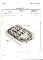
Page 18: ...ree slotted screws Item 5 as shown in Figure 9 Grasp the battery cover using the opening as a handle and gently lift the cover while pulling toward the front panel to release the tabs Remove the worn...

Page 19: ...MODEL 167 OPERATING INSTRUCTIONS FIGURE 9 Battery Installation 0172 13...

Page 20: ...oved or is less than the battery voltage the Model 167 automatically switches to battery power If no batteries are installed set the instru ment to OFF before the auxiliary power is applied to ensure...

Page 21: ...eithley Manufacturer Description Part No and Part No Alkaline D Cell BA 26 Mallory MN1300 Nickel Cadmium D Cell BA 27 Gould 4 0SCB BATTERIES INSTALLED WITH POLARITY SHOWN m LO CLIP LEAD STORED IN OPEN...

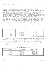
Page 22: ...n Table 3 2 The 167 downranges whenever the input goes below 1 9 0 Upranging occurs whenever the input exceeds 1 9 9 9 When the input signal exceeds 499 volts rms the display flashes on and off to ind...

Page 23: ...whenever the input goes below 1 9 0 Upranging occurs whenever the input exceeds 1 9 9 9 When the measured re sistance exceeds 19 99 Mfi the display flashes to indicate an overrange con dition TABLE 3...

Page 24: ...assembly and maintenance b Compactness and high reliability are provided through the use of a dig ital LSI a completely solid state LED display and thick film resistor net works c Low power dissipatio...

Page 25: ...sed for signal transfer for one polarity only If the Input to the rectifier Is negative QA103 provides a gain of 1 so that the output Is positive When the Input to the rectifier Is positive QA103 prov...

Page 26: ...riod over a span of 2016 counts This is accomplished by an AND gate as shown in Figure 20 For example a 1 volt input would result in a total discharge period of 1000 counts An input of 250 millivolts...

Page 27: ...multiplex OUTPUT AUTO ranger OUTRANGE DISPLAY OUTPUTS FUNCTION INPUTS FUNCTION DECODER RANGE COUNTER FUNCTION decimal POINT TO READOUTS RANGE OUTPUTS FIGURE 13 LSI Block Diagram A n CONVERTOR INTEGRAT...

Page 28: ...H Threshold input 5V or 12V 9 CS Current switch 5V integrate mode 10 TO Multiplex line 5V ON OV OFF 11 TI Multiplex line 5V ON OV OFF 12 T2 Multiplex line 5V ON OV OFF 13 T3 Multiplex line 5V ON OV OF...

Page 29: ...ic Designation Function Fl F2 ACV 1 0 DCV 1 1 DCV 0 1 OHMS 0 0 NOTE With 3 range lines R R2 and R there are 8 possible states of which four are used on ACV and DCV five on OHMS The remaining states ma...

Page 30: ...1 1 1 d dp FIGURE 15 Identification of Segments d Multiplexing Circuit The multiplexing circuit is also included in inte grated circuit QA201 The digital display is controlled by the four multiplex i...

Page 31: ...ge b Calibration Two internal adjust potentiometers R112 and R113 are used for calibrating the DCV function c Filtering In the dc mode filtering is provided by capacitor CllO in the feedback loop Addi...

Page 32: ...O I 1 200V 55 pF 50M 500K 0 0055 mF 0 01 500V 55 pF 50M 5OK 0 055 pF 001 In addition to Cj the input cable from the probe adds approx 165 pF capacity because there is a shielded coax cable inside the...

Page 33: ...etermined by the 4 5V reference voltage and the range resistor The voltage developed across the terminals is proportional to the measured resistance For example when a 15 megohm resistor is connected...

Page 34: ...ernal batteries and external supply are connected Whenever the external supply voltage is greater than the battery voltage diode D301 is back biased off If the external voltage is removed diode D301 c...

Page 35: ...l measurements should be made at ambient temper ature of approx 25 C and relative humidity below 50 If the instrument is out of specification at any point perform a complete calibration as given in Pa...

Page 36: ...too low b Accuracy Check 1 DCV Function Use Voltage Source B or equivalent test equipment a Install the probe in the front panel b Apply a dc voltage as given in Table 5 2 between HI and LO c Verify...

Page 37: ...anel b Apply a resistance as given in Table 5 4 c Verify that the reading on the display is within the tolerances stated TABLE 5 4 Accuracy Check for OHMS Source Source Input Accuracy Reading Toleranc...

Page 38: ...vary more than 12 digits from 20 Hz to 10 kHz Readings should not vary more than 24 digits from 20 Hz to 20 kHz e AC Rejection 1 Depress the DCV pushbutton 2 Install the probe in the front panel 3 App...

Page 39: ...he top cover on top of the printed circuit board such that the metal shield on the cover faces up Make a temporary connection be tween common on the circuit board and the metal shield using a clip lea...

Page 40: ...MAINTENANCE MODEL 167 FIGURE 20 Top Cover Assembly 34 0172...

Page 41: ...MODEL 167 MAINTENANCE BATTERY LEAD RED METAL SHIELD ON INSIDE TOP COVER COMMON REINSTALL PROBE AFTER COVER IS REMOVED INPUT HI INPUT LO FIGURE 21 Chassis Assembly 0172 35...

Page 42: ...just potentiometer RllO for 0 009 to 0 010 Vdc display reading g Repeat steps b through f to ensure that both adjustments are within tolerance 3 DCV Accuracy Adjust a Depress the DCV pushbutton b Appl...

Page 43: ...MODEL 167 MAINTENANCE 10V AC CAL IV AC CAL lOOV AC CAL AMPLIFIER ZERO TEST POINT TPl DC CAL 4 lOkQ CAL DISPLAY ZERO DC CAL IkQ CAL RECTIFIER ZERO INPUT ZERO FIGURE 22 Calibration Controls 0172 37...

Page 44: ...djustments in the exact sequence given so that proper cali bration of accuracy results 1 lOOV Range Adjustment This calibration also sets the 500V range a Depress the ACV pushbutton b Apply a 8 kilohe...

Page 45: ...Pin 4 should be 12V 57 If voltages missing see c below 4 Malfunction of di gital circuitry Check for supply voltages on each integrated circuit of the follow ing QA201 QA202 QA203 QA204 5 Malfunction...

Page 46: ...If TP2 0 check QA102 and QA103 4 If TP2 0 check QA104 and QA105 e Minus signal does not operate for DC input Integrated circuit QA107 Replace QA107 f One or more seg ments do not light when input is s...

Page 47: ...r battery types replace the batteries if the voltage is less than 6 volts NOTE To properly determine the battery potential the cells must be measured in the 167 with power on so that batteries are und...

Page 48: ...on the chassis toward the rear panel Make certain the tabs are fully engaged so that the 3 screw holes align properly Replace the 3 screws to complete the reassembly NOTE The Model 167 is completely p...

Page 49: ...y batteries since the cells may leak or explode b Battery Test After recharging or replacing Ni Cad cells turn on the Model 167 to verify proper operation If the instrument does not turn on check the...

Page 50: ...MAINTENANCE MODEL 167 BATT TEST COMMON 11 CLOCK M PIN 1 RMQ6 ro OHMS REF a ISft o 85 fft51 m 1 n QA2i X i L i PIN 1 I I aJ W 3 cn PIN 1 rfiiflA FIGURE 24 Test Points on Circuit Board...

Page 51: ...t number used when ordering parts from the factory Table 6 1 gives the abbreviations and symbols used in the instruction manual A manufacturer code to name listing is given in Table 6 5 6 2 ORDERING I...

Page 52: ...ircuit picofarad 10 farad ETT electrolytic tantalum farad iF 10 farad pF F piv peak inverse voltage FET field effect transistor P plug fempto poly polystyrene FL filter pot potentiometer variable resi...

Page 53: ...9 2K C116 33 C64 5P Q108 31 TG 6I R116 R76 47 C117 34 064 150P QAlOl 19 10 24 R117 R76 270K C118 28 0221 lM QA102 18 10 24 RNIOI 133 TF 6 C119 76 0228 39M QA103 12 10 42 RN102 2 TF 2 C120 107 0143 IK...

Page 54: ...82 831000X5F0 471K C22 470P 1 C113 5pF 107 lOOOV CerD 71590 DD050 10 C64 5F 3 C114 39ijF 107 15V Epoxy 17554 TD4 015 396 10 C228 39M 3 C115 39 iF 107 15V Epoxy 17554 TD4 015 396 10 C228 39M C116 5pF 1...

Page 55: ...C179 10M C311 lOpF 207 20V Tant 17554 TD2 20 106 20 C179 10M C3i2 ISOpF 107 lOOOV CerD 71590 DD151 107 C64 150P 2 C3I3 IOOOmF 25V EMC 73445 ET102X025A03 C160 1000M 1 C314 lOpF 207 20V Tant 17554 TD2...

Page 56: ...9K 1 17 1 8 W MtF 91637 MFF 1 8 T1 493 R88 49 9K 2 RI03 49 9KS1 17 1 8 W MtF 91637 MFF 1 8 T1 493 R88 49 9K RI04 20K 1 107 75 W Comp Var 73138 89PR20K RP89 20K 1 RI05 4 5KS 17 10 W WW 91637 RS 10 453...

Page 57: ...TS3538 TG 88 Q108 PNP Silicon TO 92 Case G7263 2N5087 TG 61 1 Q301 NPN TO 106 Case 12G4G 2N4355 TG 90 2 Q302 NPN TO 106 Case 1204G 2N4355 TG 90 Q303 NPN Silicon TO 92 Case 07263 2N3903 TG 49 2 Q304 NP...

Page 58: ...r ball 4 FE 6 Foam cushion 3 25191A Battery compartment 1 24620D Clips 6 24536B Probe connector 1 TJ 11 Guide probe tip 1 24624A Screw 6 32 slotted 3 25368A Circuit board Board with components 1 PC 30...

Page 59: ...ABLE PARTS R303 D308 R304 i R301 RN301 D307 RM104 D303 RNI03 R112 R115 Rill RIi3 Dice D103 D105 R107 RM302 DlOl D102 R108 D107 R106 Rm02 RllO RNlOl R104 R103 R102 RI09 SlOl FIGURE 25 Component Layout...

Page 60: ...REPLACEABLE PARTS MODEL 167 C313 C305 0302 0308 0303 0312 0118 0203 0117 0105 0112 0102 m 0113 0114 0108 FIGURE 26 Component Layout Capacitors 54 0172...

Page 61: ...MODEL 167 REPLACEABLE PARTS QA302 M QA3C1 OA105 QA104 QA201 OA102 OA204 QA202 Outline M XLFTONE LINE FIGURE 27 Component Layout Transistors QAlOl 0172 55...

Page 62: ...1 ir l g I gi 10 o I I 22 K I CO 11 1 Si l i 76 75 L 3CJ 5 USD K o Is 107 I g II a I I 67 _6 _ 68 65 I I I 10 K N 10 o o o 111 M l o 62 61 30 I o 121 Is 00 117 CJ 32 33 34 58 I 57 H 0 57 1 54 zroTi 3...

Page 63: ...ITHLEY PART NO IC 38 JEDEC TO 116 TtrararHTErEnzr g 4B 4A 4 3B 3A 3Y C 3 D 7 IV 2A 2B 2Y KEITHLEY PART NO IC 25 irai iura immnyim JEDEC TO 116 LU UJ li 111 15J16J LZJ Vf VoOT g 9 D 3 VOLTAGE REGULATOR...

Page 64: ...ij u lij lij 14J lii b 3 5 6 LEAD DESIG TO 5 E TO 5 LEAD DESIG TO 106 Eo oC B j TO 106 c BOTTOM VIEW KEITHLEY PART NO IC 53 irai na ira rm ng m Bi 13 JEDEC TO 116 D 2 3 4 5 6 LEAD DESIG TO 92 TO 92 BO...

Page 65: ...MODEL 167 REPLACEABLE PARTS f o M 1 1 1 i 1 CN r r 0 i 1 s r 8k L 0 FIGURE 31 Case Outlines 0172 59...

Page 66: ...REPLACEABLE PARTS MODEL 167 PIN 1 is flattened as shown FIGURE 32 Case Outline LSI 1 60 0172...

Page 67: ...MODEL 167 REPLACEABLE PARTS DIGITAL DISPLAY PROBE WINDOW PROBE BOARD BRACKET SCREW 4 40 FLAT HEAD BRACKET SCREW 4 40 BINDER HEAD PROBE BOTTOM FIGURE 33 Probe Assembly 0172 61...

Page 68: ...if 94086 02735 RCA 11502 IRC Inc 22525 Berg Electronics Inc Receiving Tube Div Boone N C 28607 New Cumberland Pa 17070 Somerville N J 11534 Duncan Electronics Inc 23020 General Reed Co 02777 Hopkins E...

Page 69: ...Mass Cleveland Ohio 44139 71468 ITT Cannon Electric Inc 93656 Electric Cord Co Los Angeles Calif 90031 80294 Bourns Inc Caldwell N J Riverside Calif 92506 71590 Centralab 94144 Raytheon Co Industrial...

Page 70: ...uxiliary Power connections and battery supply The Fush to Read switch is shown on Block Diagram No 25354D c Analog Circuit No 25342D This diagram shows the circuitry used in the analog amplifier and r...

Page 71: ...capacitor fixed or variable diode pn junction diode zener reference Inductor fixed transformer fixed amplifier Integrated circuit type transistor npn type battery single cell transistor field effect F...

Page 72: ...ES fsfle i C ATHOPES 0464 d4 i U dp S CATH0D 3 OPEN NO CONNECTIONS di d s d3 d t ANODES 03 t ANODES I FRONT PANEL OPEN NO CONNECT IONS CLi 02 d3 U4 ANODES fi f2 f3J i ANODES a 2 pp CATh40DE5 24604C CA...

Page 73: ...2 3 SoAAA O 5 77K C30I RN302 14 3 K 0304 RN30I 5 II3K 0 5V BT305 0307 RN30 4 aoT C304 t BT30e 0309 a C3I4 10 1000 P303 R303 39 ojoe CND RN308 f J4 3K CJ08 RN 301 3 47K OA 30 o clock RN30I 9 t8K L308 d...

Page 74: ...O PA 0J 4 RNI03 5 o w o o l2 HIGHEST SCHEMAnt DEStCNATiONS USED A A DI08 RNlOf QAI07 SCHEMATIC DESIGNATIONS NOT USED OF ALL RESISTANCE CAPACITANCE SHALL BE DESIGNATED IN OHMS MICROFARADS UNLESS OTHERW...

Page 75: ...POUUER SUPPLY 0PUUC 25340D J20I QAJ03 C204 00 203 001 202 001 I I 20 00 ICHE5T SCHEMATIC DtSiCN sriONS USED NOTES ALL CAPACITANCE SHALL BE DESIGNATED IN MICROFARADS UNLESS OTHERWISE NOTED Digital circ...

Page 76: ...opriate box Alkaline batteries installed I I Rechargeable Nickel Cadmium batteries installed I I Model I67I Recharger utilized I I Line operation using Model 1672 I17V I I 234V I I External power sour...

Reviews: