background image

(TE2)

330k

10pF

(VC)

Oscilloscope

+

-

8

DM-S500

ADJUSTMENT

4. Press the PLAY key to display “EFBAL MO-W” and after

that press the PLAY key again to display
"EF=$##MOW".

5.  Turn the SHUTTLE so that the waveform on the

oscilloscope satisfies the specified value. (When the
SHUTTLE is turned, the #-marked figure in "EF=$##"
changes and the waveform also changes.)During this
adjustment, the oscilloscope changes in units of about
3%.  Adjust so that the waveform comes nearest to the
specified value. (MO groove read power traverse
adjustment)

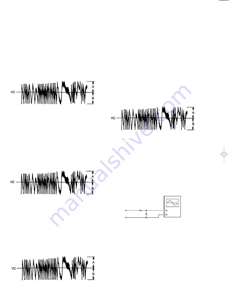
(Traverse waveform)

Specification : A = B

6. Press the PLAY key to display "EFB=##XSA"

momentarily. After that, "EF=$##MOR" is displayed.
(Laser power READ power, forcus servo ON, tracking
servo OFF, and spindle(S) servo ON.)

7.  Turn the SHUTTLE so that the waveform on the

oscilloscope satisfies the specified value. (When the
SHUTTLE is turned, the #-marked figure in "EF-##"
changes and the waveform also changes.) During this
adjustment, the oscilloscope changes in units of about
2%. Adjust so that the waveform comes nearest to the
specified value. (MO groove read power traverse
adjustment)

(Traverse waveform)

Specification : A = B

8. Press the PLAY key to display “EFB=##XSA”

momentarily and save the adjustment result in
nonvolatile memory  After that, "EFBAL MO-P" is
displayed.

9.   Press PLAY key to display "EF=$##MOP".(A pick-up

moves automatically to pit block area.)

10. Turn the SHUTTLE so that the waveform on the

oscilloscope comes near to the specified value.  During
this adjustment, the waveform changes in units of about
2%.  Adjust so that the waveform comes nearest to the
specified value.

(Traverse waveform)

Specification : A = B

11. Press the PLAY key to display “EFB=##XSA”

momentarily and save the adjustment result in
nonvolatile memory.  After that, “EFBAL CHAN” is
displayed.  The disc rotation stops automatically.

Note : The "#" display on the screen indicates an arbitrary

figure.

12. Press the EJECT key to take out a recordable disc.
13. Insert test disc TGYS-1.
14. Press the PLAY key to display “EF=$##CD”.  A servo is

established automatically.

15. Turn the SHUTTLE so that the waveform on the

oscilloscope comes near to the specified value.  During
this adjustment, the waveform changes in units of about
2%.  Adjust so that the waveform comes nearest to the
specified value.

(Traverse waveform)

Specification : A = B

16. Press the PLAY key to display “EFB=##XSA”

momentarily and save the adjustment result in
nonvolatile memory.  After that, “EFBAL ADJU” is
displayed.

17. Press the EJECT key to take out test disc TGYS-1.

Notes :
1. Data is erased during MO write when a recorded disc is

used for this adjustment.

2. If the traverse waveform is difficult to be monitored,

connect an oscilloscope as shown in the figure below.

3-7 Focus bias adjustment

Connection :
1. Insert a continuously recorded disc (refer to 3-4,

“Creating the recordable continuous recording disc”).

2. Turn the SHUTTLE to display “CPLAY MODE”.
3. Press the PLAY key to display “CPLAY MID”.
4. Press the STOP key when "C=

✽ ✽ ✽ ✽

a=

✽ ✽

" is

displayed.

5. Turn the SHUTTLE to display “FBIAS ADJU”.
6. Press the PLAY key to display “a=## ####/”.  The four-

digit figure indicates the C1 error rate, and the two-digit
figure after “a=” indicates the focus bias value.

DM-S500 

EXP 


98.4.26 

2:41 

PM 

  y [ W  2

Summary of Contents for DM-S500

Page 1: ...Dressing panel A21 3621 03 Indicator B12 0329 04 Miniature phone jack E11 0188 05 AC power cord E30 Optic receiving module W02 1181 05 Power cord bushing J42 0083 05 Phono jack E68 0120 05 Metallic cabinet A01 3444 01 Front glass B10 2386 12 Knob K29 6835 12 Knob K29 6835 12 Knob K29 6835 12 Knob K29 6945 04 Panel A60 In compliance with Federal Regulations following are reproduc tions of labels on...

Page 2: ...and movement Before transporting or moving this unit carry out the following operations 1 With no disc loaded in the unit press the ON STANDBY key to on Check that no disc is present in the unit 2 Wait a few seconds and verify that the display shown appears 3 Press the ON STANDBY key to off standby dB N O I D I S C R L 3 0 1 30 10 5 Cleaning Unplug this appliance from the wall outlet before cleani...

Page 3: ...e 4 TIME DISPLAY key 5 Mini Disc insertionslot Insert a minidisc 6 Eject 0 key Press to unload the Mini Disc 7 SHUTTLE 4 knob Use to skip disc tracks during playback During editing this knob is used to select track numbers title and characters 8 REC LEVELkeys This key is used to adjust the recording level 9 REC INPUT key This key is used to switch the recording input source 0 REC key Press when st...

Page 4: ...TOR TITLE INPUT CURSOR CHECK AUTO MANU TITLE SEARCH 4 EDIT CANCEL 7 3 1 8 REMOTE CONTROL UNIT RC M0502 1 2 6 7 8 3 4 9 5 1Segment screen This screen is used for selecting the icons for the main equip ment Graphical Remote Control Unit GRC REMOTE CONTROL UNIT ON STANDBY MUTE VOLUME ENTER Return VCR2 VCR1 TV Sat Cable TapeB TapeA Confirm Tape1 LD MD DVD Tuner CD Set Up Main Menu MD Edit Mode PGM 10k...

Page 5: ...est mode While pressing the PLAY key plug the AC power cord into he AC wall outlet 2 2 Canceling the test mode Unplug the AC power cord 1 Test mode of the unit 2 3 Basic operation in test mode All operations are performed using the SHUTTEL up down PLAY key and STOP key The functions of each key are shown in the table below 2 4 Selection of test mode 12 test modes are selected by turning the SHUTTL...

Page 6: ...Notice that recording is performed irrespective of the erasure prevention control position when the REC key is pressed 2 6 Precaution on use of test mode An erasure prevention control is not detected in the test mode Therefore when the recording laser power mode such as continuous recording mode and traverse adjust ment mode is entered the contents of the existing recording are erased irrespective...

Page 7: ...the PLAY key to display 0 9mW 4 Adjust to turn SHUTTLE so that the laser power meter reads 0 86 0 94mW Set range 10mW of the laser power meter then save to press PLAY key 5 7 0mW is displayed 6 Adjust to turn the SHUTTLE so that laser power meter reads 6 9 7 1mW then save to press PLAY key LDPWR is displayed momentarily Don t output the laser power of 7 0mW more than 15sec 7 Next turn the SHUTTLE ...

Page 8: ...he waveform changes in units of about 2 Adjust so that the waveform comes nearest to the specified value Traverse waveform Specification A B 11 Press the PLAY key to display EFB XSA momentarily and save the adjustment result in nonvolatile memory After that EFBAL CHAN is displayed The disc rotation stops automatically Note The display on the screen indicates an arbitrary figure 12 Press the EJECT ...

Page 9: ... by calculation 2 The C1 error rate fluctuates Therefore perform the adjustment according to the observed mean value C1 error Focus bias value 3 8 Error rate confirmation 3 8 1 CD error rate confirmation Confirmation 1 Insert test disc TGYS 1 2 Turn the SHUTTLE to display CPLAY MODE 3 Press the PLAY key to display CPLAY MID 4 C a is displayed 5 Confirm that the C1 error rate is less than 20 6 Pres...

Page 10: ...10 1 E A C B D 2 3 5 7 4 6 PC BOARD Component side view Refer to the schematic diagram for the value of resistors and capacitors MD MECHANISM UNIT MD CONTROL UNIT ...

Page 11: ...2 3 2 2 1 1 5 2 6 B R33 R34 B E Q6 R32 C16 R30 C19 C20 C21 R35 R31 C7 R29 R9 R10 R26 C9 R27 R3 R2 R1 16 1 33 48 32 49 17 64 R23 B E Q5 IC1 C4 C2 C3 R15 C6 R40 R37 R36 R20 R18 R4 R8 R11 R19 R5 R25 C17 R6 R14 R13 R12 R16 R17 R28 R7 C18 C8 B E Q1 F G I K M O H J L N Refer to the schematic diagram for the value of resistors and capacitors C BOARD Component side view 12 PCB SD 98 4 263 43PM y W 4 ...

Page 12: ...5 4 A A A 2 100u 6 3 C136 L11 0 1 C135 100 R137 4700P C133 C131 0 015 R140 150 1K R134 C132 0 47 C112 4700P C113 1 4 5 2 3 1 6800P 0 01 C105 470K R117 R106 3 3M L10 L5 L6 L9 R108 1K R109 1K 10u10 C119 R185 10K 47K R179 10u10 C101 C102 0 1 R190 10K 0 033 C189 100K R159 C158 R158 100K 10K R188 10K R189 3 3K R177 3 3K R175 L1 10uH 10u10 C161 100uH L4 92 91 89 88 18 17 16 0 22 10K 10K R184 C188 0 01 R...

Page 13: ... LRLH NMUTE NC NC GND VDD NC 8FSBCKO 8FSLDATAO 8FSRDATAO 8FSWCKO NC NC TEST1 TEST0 BCKO DATAO LRCKO NRSTO GND 46 47 48 49 50 51 52 53 54 55 56 57 58 59 60 30 29 28 27 26 25 24 23 22 21 20 19 18 17 16 27 FIL 25 24 21 22 23 GND 5V FIL H GND ADDT H 5V 26 18 19 15 16 17 OCLK VLLAT VLDATA U GND DOUT 14 F OFF 5V 20 13 10 11 12 71 40 72 11 12 SCK SDAC 8FS 45 44 43 42 41 40 39 38 37 36 35 34 33 32 31 1 2 ...

Page 14: ... VCO VIN AGND R AVDD NC 37 38 39 40 41 42 43 44 45 46 47 48 24 23 22 21 20 19 18 17 16 15 14 13 LRCK DATAOUT BCLK SUB2 SUB1 DGND ERROR CLKOUT2 CLKOUT1 XOUT XIN DVDD DOUT V ENPHA RC1 RC2 CCB SUB DGND CLKND CLK TEST1 TEST2 XMODE DVDD 36 35 34 33 32 31 30 29 28 27 26 25 1 2 3 4 5 6 7 8 9 10 11 12 77 D C 2SA954 2SC2003 2SA1048 2SC2458 2SA1309A 2SC3311A FMW1 TA8409S NJM062M NJM2115M BU4094BCF TC74HCT70...

Page 15: ...2 VCC 82 R123 2 2uH 22P 180 R122 6P C122 R121 10 8 7 GND 9 11 10 12 14 13 4 7u35 C114 C113 0 1 0 01 C115 11 1 10K R21 R22 10K 14 13 12 10 9 7 6 8 11 4 5 3 2 1 15 SDT1 SDT0 16 DEM0 MCLK SCLK 17 DEM1 LRCK 19 TST3 DIF0 20 TST1 TST2 DIF1 AGND 22 VD AINL 23 PWDA DGND VA 21 18 AINL PWAD AINR AINR AOUTL CMODE 26 25 24 VREFL AOUTR VREFH VCOM 28 27 C25 10u25 C26 10u25 R24 56K 470 R18 R17 470 0 01 C107 C108...

Page 16: ... 60 RES 61 47K U 5V OSCO 9 10 6 7 8 AM6 AM5 AM8 AM7 AM9 AM10 3 5 4 1 2 AM3 AM2 AM1 AM4 CE 62 CL 100 R37 63 DI R36 100 16 14 15 11 12 13 8 9 10 5 6 7 3 4 1 2 R12 10K R13 10K R14 10K C2 0 47 0 1 TEST 10u35 115V M 230V E M W101 WH3 BLUE WH5 YELLOW WH4 RED HOT COLD R39 2 2 1 4W R38 2 2 1 4W 50V 50V 18V 7 5V 7 5V GND B 7 5V FIRST OFF F F 1 2 3 4 5 6 C15 4 7u35 R24 1 5K 1 4W C14 22u63 34 33 AM33 AM34 36...

Page 17: ... 2 37 7 24 1 4 34 21 48 10 47 5 27 26 15 16 22 36 35 12 23 41 48 LM DM FM 43 29 29 40 29 29 13 11 RH 8 49 42 B A 27 26 18 AE AF AG AH M1 7x4 5 ø2x4 ø2x8 ø2 6x6 BLK N39 1745 46 N82 2004 46 N89 2008 46 N89 2606 45 The figure which was seen from below Slit When assembling a mechanism adjust slit A and slit B of the main slider Ref No 18 and the main gear Ref No 27 A B Parts with exploded view numbers...

Page 18: ...Cx2 Cx2 C C C C C C C A B C D E F ø2 6x8 ø3x6 ø3x8 BLK ø2 6x6 BLK ø3x18 ø4x8 N82 2608 46 N89 3006 46 N89 3008 45 N89 2606 45 N89 3018 46 N09 1729 05 601 658 632 654 651x3 646 646 652x2 650x2 650x2 665 618 653 661 608 610 663 615 606 607 605 616 645 660 634 29P 636 27P 637 13P 637 13P 662 3 3 662 2 3 620 1 2 620 2 2 662 1 3 634 29P 635 19P 635 19P 602 611 770 631 630 633 619 D D 774 774 773 774 703...

Page 19: ...1 10W R6 RK73FB2A432J CHIP R 4 3K J 1 10W R7 RK73FB2A822J CHIP R 8 2K J 1 10W R8 RK73FB2A103J CHIP R 10K J 1 10W R9 RK73FB2A242J CHIP R 2 4K J 1 10W R10 RK73FB2A432J CHIP R 4 3K J 1 10W R11 14 RK73FB2A103J CHIP R 10K J 1 10W R15 RK73FB2A104J CHIP R 100K J 1 10W R16 RK73FB2A103J CHIP R 10K J 1 10W R17 RK73FB2A472J CHIP R 4 7K J 1 10W R18 19 RK73FB2A242J CHIP R 2 4K J 1 10W R20 RK73FB2A432J CHIP R 4...

Page 20: ... 0 010UF K C225 CK73FF1C224Z CHIP C 0 22UF Z C226 227 CK73FB1H103K CHIP C 0 010UF K C251 CK73FB1H102K CHIP C 1000PF K C252 CK73FB1H103K CHIP C 0 010UF K C253 CC73FSL1H101J CHIP C 100PF J C254 255 CK73FB1H103K CHIP C 0 010UF K C256 CK73FB1E104K CHIP C 0 10UF K C257 CK73FB1H103K CHIP C 0 010UF K C258 CK73FB1C224K CHIP C 0 22UF K C259 CK73FB1H103K CHIP C 0 010UF K C261 CE04KW0J331M ELECTRO 330UF 6 3W...

Page 21: ...2A331J CHIP R 330 J 1 10W R283 284 RK73FB2A104J CHIP R 100K J 1 10W R285 RK73FB2A473J CHIP R 47K J 1 10W R286 RK73FB2A104J CHIP R 100K J 1 10W R287 RK73FB2A472J CHIP R 4 7K J 1 10W R288 RK73FB2A473J CHIP R 47K J 1 10W R289 RK73FB2A101J CHIP R 100 J 1 10W R290 RK73FB2A471J CHIP R 470 J 1 10W R291 RK73FB2A104J CHIP R 100K J 1 10W R292 RK73FB2A102J CHIP R 1 0K J 1 10W R293 294 RK73FB2A103J CHIP R 10K...

Page 22: ...B1C224K CHIP C 0 22UF K C116 CK73FB1H223K CHIP C 0 022UF K C117 118 CK73FB1E104K CHIP C 0 10UF K C119 C92 0628 05 CHIP TAN 10UF 10WV C121 C92 0048 05 ELECTRO 100UF 6 3WV C122 CK73FB1H103K CHIP C 0 010UF K C123 CK73FF1E104Z CHIP C 0 10UF Z C127 CK73FF1E104Z CHIP C 0 10UF Z C128 CK73FB1H103K CHIP C 0 010UF K C129 CK73FB1C474K CHIP C 0 47UF K R295 RK73FB2A473J CHIP R 47K J 1 10W R301 RK73FB2A333J CHI...

Page 23: ...5 TC74ACT540FS MOS IC IC6 X24C01AS 2 7 MEMORY IC IC7 HM51W4400BTT 7 MEMORY IC IC8 BH6511FS ANALOGUE IC IC10 L88MS33T ANALOGUE IC Q1 FMW1 TRANSISTOR Q2 3 DTA144EUA DIGITAL TRANSISTOR Q4 5 DTC114YUA DIGITAL TRANSISTOR Q6 2SA1576A R S TRANSISTOR Q7 2SB798 DL TRANSISTOR C130 CC73FSL1H101J CHIP C 100PF J C131 CK73FB1H153K CHIP C 0 015UF K C132 CK73FB1C474K CHIP C 0 47UF K C133 CK73FB1H472K CHIP C 4700P...

Page 24: ...EXTENSION SP S HD 34 2A G01 4014 08 EXTENSION SP DOOR 35 3B G10 0146 04 NON WOVEN FABRIC 36 2B N19 1101 04 POLY WS 1 2 3 0 0 5CUT 37 1B N19 1105 04 POLY WS 1 6 3 5 0 5CUT 38 1A N19 0366 04 POLY WS 2 1 4 0 0 5CUT 39 1A G16 0877 04 SHEET TRAY 40 2B E35 1715 08 WIRING HARNESS 41 3A E35 1780 08 FLAT CABLE 42 3B J80 0012 08 FPC 47 2B S33 1022 05 PUSH SWITCH SPPB12 48 2A 3A J26 0052 08 PCB ASSY X29 2580...

Reviews: