DP-1100B II
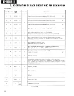
2. IC OPERATION OF EACH CIRCUIT AND PIN DESCRIPTION
Pin f u n c t i o n s
Pin No.
Symbol
I/O
W a v e f o r m
Description
Remarks
27, 61
-
-
Voltage supply pin
2 8 , 6 2 ,
67
-
\
GND pin
2
PBFS
I
—
Frame sync input. The symbol data period signal of each frame sent
from TC9178F (IC8) is input.
Connected to PBFS
(pin 56) of TC9178F
(IC8)
3
MWRE
I
—
Memory write request input which accepts MWRE signal from
TC9178F (IC8)
Connected to MWRE
(pin 67) of TC9178F
(IC8)
4
BOEN
0
-
Output enable. When signal MWRE from TC9178F (IC8) can be ac
cepted, the control signal to release symbol data output DBOO to
DB07 from Hi-impedance state is output.
Connected to BUSE
(pin 66) of TC9178F
(IC8)
5 - 1 4 ,
18
AD0—AD9,
A D 1 0
0
\ 5 V
0.2
/ OV
External RAM address data output. Connected to address data input
of external RAM.
5 - 1 4 ,
18
AD0—AD9,
A D 1 0
0
1
0.
MS
\ 5 V
0.2
/ OV
External RAM address data output. Connected to address data input
of external RAM.
15
R/W
0
ft
3.4 nS
Read/write signal output to external RAM. Connected to R/W input of
external RAM.
" L " = Read, " H " = Write
16
CE2
0
Chip enable 2 signal is output when external RAM is read or written.
Connected to CE2 input of external RAM.
Not connected
17
CE1
0
0.48 nS
Chip enable 1 signal is output when external RAM is read or written.
Connected to CE1 input of external RAM.
1 9 - 2 6
I / 0 - 7 -
l/O-O
I/O
Data bus line connected to l/O-O to 7 of external RAM and DB04
-DB07.
1 9 - 2 6
I / 0 - 7 -
l/O-O
I/O
J0.2 /tS
Data bus line connected to l/O-O to 7 of external RAM and DB04
-DB07.
1 9 - 2 6
I / 0 - 7 -
l/O-O
I/O
\ / u V
1 nS
Data bus line connected to l/O-O to 7 of external RAM and DB04
-DB07.
T a b l e 2 - 3 - 4 A
92
Summary of Contents for DP-1100 B
Page 3: ...D P 1 1 0 0 B II D P 1 1 0 0 B II I BLOCK DIAGRAM ...
Page 32: ...D P 1 1 0 0 B II 1 CIRCUIT DESCRIPTION Disc Scratch Dust RFES D C O N D O C K Fig 1 2A 3 5 ...
Page 112: ...2 IC OPERATION OF EACH CIRCUIT AND D P 1 1 0 0 B II PIN DESCRIPTION Fig 2 4 1 G 1 ...
Page 117: ...DP 1100B II I OPERATION OF MAIN MICROPROCESSOR Fig 3 1D Q data reading flow chart ...


