DV-5050M/5900M/DVF-J6050/J6050-G
21
CIRCUIT DESCRIPTION
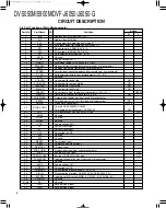
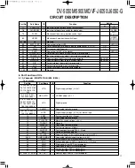
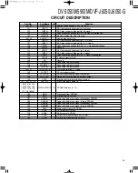
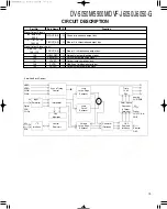
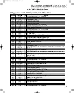
Port No.
Port Name
I/O
Function
91
VSYNC/CREFO
O
Vertical sync output. This signal provides the vertical sync function
for the outputs.
92
H/CSYNCO
O
Horizontal or composite sync output. This signal provides the horizontal sync
function for the outputs.
110
FILM
O
Film mode detector output.
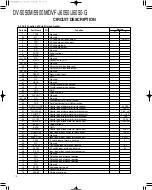
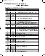
SDRAM Interface Signals
125~131
ADDR(4~10)
SDRAM address bus. This signal bus is used to address
133~136
ADDR(0~3)
-
the external SDARM(s) used for field memories.
139~143,146~150
DATA(0~4)
SDRAM data bus. This signal bus is used to transfer the data to and from
153~157,160~166
5~9,10~14,
-
the external SDRAM(s) used for field memories.
169~176
15~21,22~29
118
MEMCLKO
O
SDRAM clock and 2x output sampling clock.
119
WEN
-
SDRAM write enable. This active low signal should be connected
to the WE pin(s) on the SDRAM(s).
120
RASN
-
SDRAM row address select. This active low signal should be connected to
the RAS pin(s) on the SDRAM(s).
121
CASN
-
SDRAM column address select. This active low signal should be connected to
the CAS pin(s) on the SDRAM(s).
122
BSEL
-
SDRAM bank select.
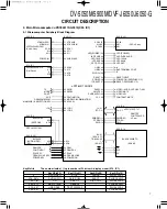
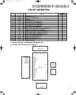
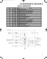
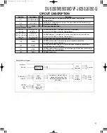
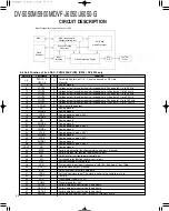
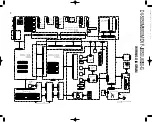
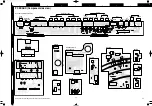
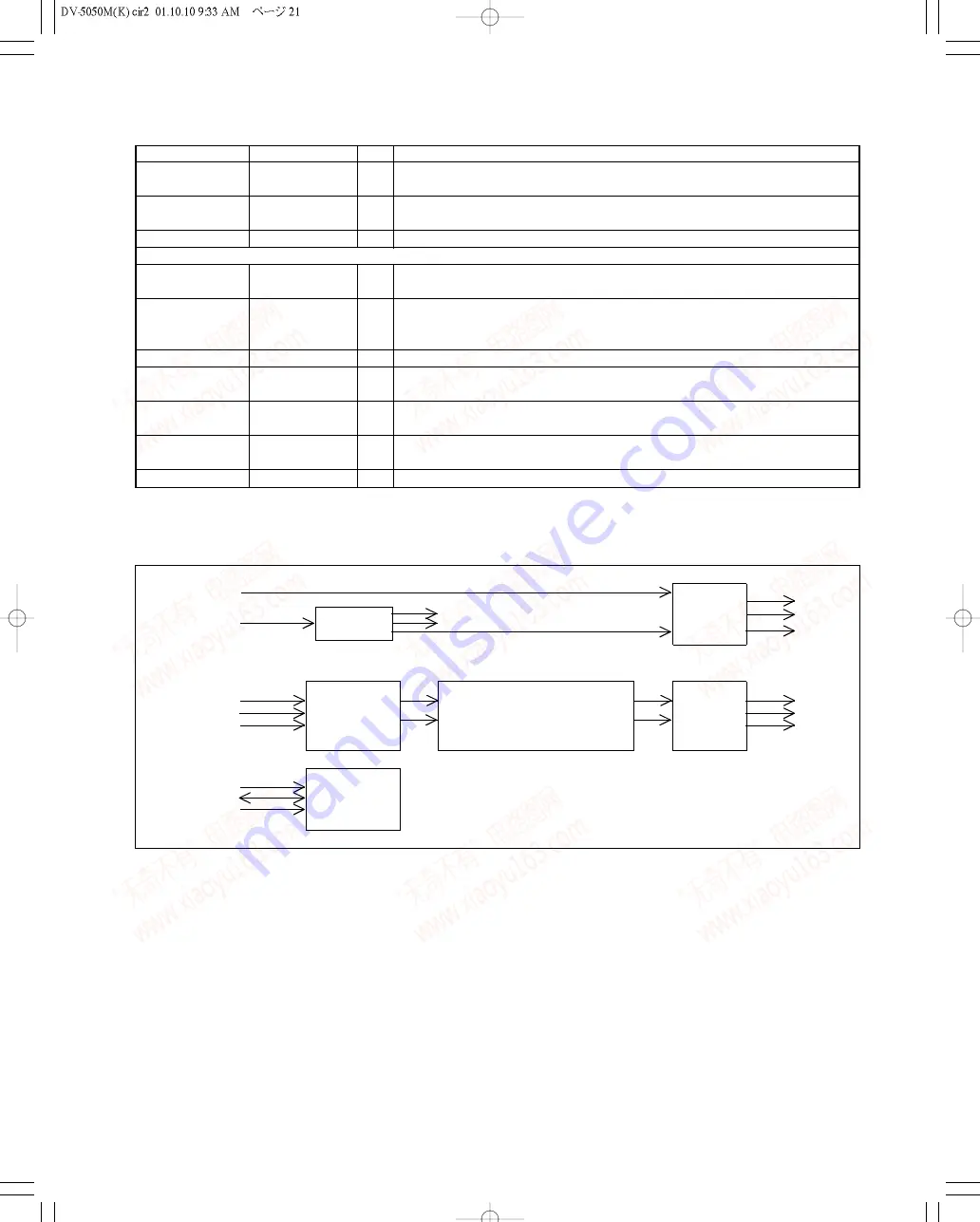
• Simplified Block Diagram
Ext. Syncs
/
PIXCLK
PLL/Clock
Generator
Sync
Generator
Sync Out
RGB/YUV/Y
CrCb/D1
10
/
/
/
Input
Signal
Formatter
Deinterlacer Core with DCDi
TM
,
Motion Compensation, Film
Mode Detection and Bad Edit
Correction
Output
Signal
Formatter
10
/
/
/
YU V
/RGB/
YCrCb
Control
Interface and
Registers
PLl/Clock
Generator
www. xiaoyu163. com
QQ 376315150
9
9
2
8
9
4
2
9
8
TEL 13942296513
9
9
2
8
9
4
2
9
8
0
5
1
5
1
3
6
7
3
Q
Q
TEL 13942296513 QQ 376315150 892498299
TEL 13942296513 QQ 376315150 892498299

