background image

AE

AG

AI

AF

AH

2

1

3

5

7

4

6

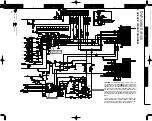
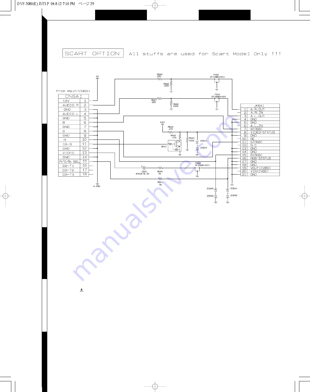
6. SCART CIRCUIT DIAGRAM

KRC103M

MTZJ13B

MTZJ13B

MTZJ5.6B

MTZJ5.6B

MTZJ5.6B

MTZJ5.6B

29

DVF-3080-S/8100

CAUTION:

For continued safety, replace safety critical com-

ponents only with manufacturer's recommended parts (refer
to parts list).

indicates safety critical components. For

continued protection against risk of fire, replace only with
same type and rating fuse(s). To reduce the risk of electric
shock, leakage-current or resistance measurements shall be
carried out (exposed parts are acceptably insulated from the
supply circuit) before the appliance is returned to the cus-
tomer.

The DC voltage is an actual reading measured with a high
impedance type voltmeter with no signal input. The mea-
surement value may vary depending on the measuring
instruments used or on the product.

Summary of Contents for DVF-3080-S

Page 1: ...0 In compliance with Federal Regulations following are repro duction of labels on or inside the product relating to laser product safety KENWOOD Corp certifies this equipment conforms to DHHS Regulations No 21 CFR 1040 10 Chapter 1 subchapter J DANGER Laser radiation when open and interlock defeated AVOID DIRECT EXPOSURE TO BEAM Caution No connection of ground line if disassemble the unit Please c...

Page 2: ...een this unit and the outside This unit may not function properly if condensation occurs In this case leave the unit for a few hours and restart the operation after the condensa tion has dried up Be specially cautious against condensation in the following circum stances When this unit is carried from one place to another across a large difference in temperature when the humidity in the room where ...

Page 3: ...jected about 15 20mm 2 Pull the Tray Disc until it is separated from the Base Main completely Fig How to Reset Parental Lock 1 Connect the TV set to DVF 3080 2 Push the power switch of DVF 3080 to be on 3 Check the display of DVF 3080 shown NO DISC 4 Push the SETUP key of remote control and TV has set up menu 5 Select the 16 9 on TV 6 Push key 1 3 9 7 1 3 9 and ENTER Push key again if mistype 7 Pu...

Page 4: ... VIDEO BUFFER IECDAOUT COAXIAL SPDI D2_T 1 3 SCART_16 9 RGB_SEL 3V3M CDLD DVDLD SVREF21 5V 8V HOMESW INSW OUTSW ROMDATA 0 7 5 2VA IC901 GMS81C2012 Hynix Front Micom POWER BOARD VFD_RXD S_REQ 5 2VA 8V DMUTE IIC VFD DAC_SCK IC503 1M 16BIT 4Bank SDRAM VD33D IIC VFD DAC_TXD 12V 5V YC_MIX VIDEO_SW SER3 DAC_ML0 OPEN CLOSE SLEGP SPINDLE FOCUS TRACK SVREF IC506 74LCX373 VD33D GPOPALE DAC_RST DMUTE D2_T 1 ...

Page 5: ...1 ALI M3355 DVDPLAYER COMBO CHIP MD IC201 IP4504 Motor Driver IC503 64M SDRAM FLASH ROM EEP ROM DVDLD CDLD CD_DVD DVDMDI CDMDI SVREF21 DVD A B C D RFO CD A B C D E F RFO SLEGP SPINDLE FOCUS TRACK DRVSB CLOSE OPEN SVREF15 FOCUS FOCUS TRACK TRACK SPINDLE SPINDLE SLED SLED LOAD LOAD OPENSW CLOSESW LIMITSW MA 0 11 DQM CLK CS CAS RAS WE MD 0 15 IIC VFD DAC_SCK IIC VFD DAC_TXD ROMAD 0 21 ROMRD ROMWR ROM...

Page 6: ...K DACCLK DAC_RST SER 0 3 DAC_ML0 VIDEO Interface AUDIO Interface Pickup DVD MD1 CD MDI SVREF21 DVD A B C D RFO CD A B C D E F RFO F F T T CD_DVD DVDLD CDLD IIC VFD DAC_CLK IIC VFD DAC_TXD MRESET S_REQ VFD_RXD X501 27MHz BA1 BA0 CSJ RASJ CASJ WEJ DGM DMCLK MD0 15 MA0 11 MPEG RGB YPbPr CVBS COMPONENT Y Pb Pr SCART RGB CVBS IC604 VIDEO 6dB Amp IC601 AUDIO DAC 2CH IC602 OP Amp LPF Buffer AUDIO R AUDIO...

Page 7: ...Assembly Up Down Belt Loading Gear Pulley Gear Loading Guide Up Down PWB Assembly Loading Base Main 4 Screws 1 Connector 1 Locking Tabs 1 Screw 1 Screw 1 Locking Tab 1 Locking Tab 1 Locking Tab 1 Hook 2Screw 2 Locking Tabs 4 1 4 1 4 1 4 1 4 1 4 2 4 3 4 3 4 3 4 3 4 3 4 4 4 4 4 4 4 4 4 4 4 4 4 4 Bottom Bottom Procedure Parts Fixing Type Fig ure Disass embly Note When reassembling perform the procedu...

Page 8: ... Clamp 1 Turn the Plate Clamp to counterclockwise direction and then lift up the Plate Clamp 1 1 2 Magnet Clamp 1 1 3 Clamp Upper 2 Tray Disc Fig 4 2 1 Insert and push a Driver in the emergency eject hole A at the right side or put the Driver on the Lever B of the Gear Emergency and pull the Lever B in direction of arrow so that the Tray Disc is ejected about 15 20mm 2 Pull the Tray Disc until it ...

Page 9: ...100 9 DECK MECHANISM DISASSEMBLY 3 Base Assembly Sled Fig 4 3 1 Release 4 Screw S2 2 Disconnect the FFC Connector C1 3 1 Gear Feed 3 2 Gear Middle 3 3 Gear Rack 1 Release the Scerw S3 4 Rubber Rear Fig 4 3 Fig 4 3 ...

Page 10: ...4 1 Unlock the Locking Tab L4 in direction of arrow B and then separate the Gear Pulley from the Base Main 8 Gear Loading Fig 4 4 9 Guide Up Down Fig 4 4 1 Move the Guide Up Down in direction of arrow A as Fig A 2 Push the Locking Tab L5 down and then lift up the Guide Up Down to separate it from the Base Main When reassembling place the Guide Up Down as Fig C and move it in direction arrow B unti...

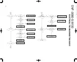
Page 11: ...ey 1 Execute Pressed Key and IR Key 2 System operation on routine loop 1 Stop playback and open tray 2 Display tray open message and LOGO Receive close key no yes no yes no yes no yes No 5V_A No 5 2VA Is 5 2VA section working Is 5 2V present at emitter of Q107 Replace Q107 Is there a DC voltage At terminal of BD101 Is there a DC voltage at R101 Replace IC101 note This Trobleshooting has various in...

Page 12: ...OSE switch Normal TRCLOSE TROPEN signal NO Check the Tray control IO pins on M3355 Normal LOAD LOAD signal NO Check the Tray control amplifying circuit on Motor driver IC201 Check the cable connection between main PCBA and loader MECHA Check AV cable connection to TV set NO YES YES YES Test Check the AC Voltage 110V or 220V Switch on the Power PCBA Check the Power PART Is the DC Voltage Outputs OK...

Page 13: ...circuit on M3355 Proper RF signal Check the related circuit on M3355 RF signal Check the RF connection between MD and M3355 Yes Yes Yes Yes Yes Yes Yes No No No No No No No Does the SLED move to inner side when it is at outer position on B Yes Motor Driver DRVSB Pin is High Check the connection line of DRVSB signal Motor Driver DRVSB Pin is High Check the related circuit of FOCUS SLED and SLED out...

Page 14: ... Yes Normal IR VFD Front panel key functions Yes Yes No No No No No Yes Yes Yes Focus ON OK D Yes Proper signals on A B C D of M3355 Check the related circuit on M3355 SBAD signal No No Check the related circuit on M3355 Proper SBAD signal on M3355 Check connections between M3355 and pick up head Track On OK Check cable connection on pick up head Proper tracking signal on M3355 Proper M3355 track ...

Page 15: ...Vp p 3 3V FIG 2 1 1 Tray open close waveform FIG 3 1 2 Tray open waveform OPEN CN203 PIN3 CLOSE CN203 PIN4 LM IC201 PIN14 LM IC201 PIN13 FIG 3 2 OPEN CN203 PIN3 CLOSE CN203 PIN4 LM IC201 PIN14 LM IC201 PIN13 3 Tray close waveform FIG 3 3 4 SLED CONTROL SIGNAL NO DISC CONDITION RELATED SLEGP 2 1V 1 5V 0 85V IC501 PIN80 DRVSB 3 3V 0V IC501 PIN22 SLED 7 3V 4V 2 4V IC201 PIN16 SLED 7 3V 4V 2 4V IC201 ...

Page 16: ...1 PIN15 FE IC501 PIN27 SBAD IC501 PIN14 FIG 7 2 DVD F CN201 PIN15 FE IC501 PIN27 SBAD IC501 PIN14 FIG 7 3 CD F CN201 PIN15 FE IC501 PIN27 SBAD IC501 PIN14 FIG 7 4 CD F CN201 PIN15 FE IC501 PIN27 F CN201 PIN18 FOCUS IC501 PIN76 FIG 8 1 DVD 8 FOCUS ON WAVEFORM F CN201 PIN15 FE IC501 PIN27 F CN201 PIN18 FOCUS IC501 PIN76 FIG 8 2 CD 9 SPINDLE CONTROL NO DISC CONDITION WAVEFORM SPM 5 5V 4V 1 5V CN202 P...

Page 17: ...KING CONTROL SIGNAL System checking RELATED 12 M3355 AUDIO OPTICAL AND COAXIAL OUTPUT ASPDIF 11 RF WAVEFORM RF IC501 PIN61 1 4V 2 95V FIG 11 1 IECDAOUT IC501 PIN211 FIG 12 1 2 Y Jk601 pin7 1V FIG 13 2 13 M3355 VIDEO OUTPUT WAVEFORM 1 Full colorbar signal CVBS Jk601 pin6 1V FIG 13 1 14 AUDIO OUTPUT FROM AUDIO DAC 3 C JK601 PIN8 0 7V FIG 13 3 1 AUDIO L R JK601 PIN4 5 1KHz 0DB FIG 14 1 ...

Page 18: ...DVF 3080 S 8100 18 WAVEFORMS 2 Audio Related Signal SER3 IC501 PIN167 BCLK IC501 PIN170 2 312MHz LRCLK IC501 PIN168 48KHz FIG 14 2 ...

Page 19: ...19 Refer to the schematic diagram for the value of resistors and capacitors PC BOARD A C E B D 2 1 3 5 7 4 6 1 MAIN P C BOARD ...

Page 20: ... to the schematic diagram for the value of resistors and capacitors PC BOARD F G I H J 2 1 3 5 7 4 6 4 SMPS P C BOARD 2 KEY P C BOARD 3 FRONT P C BOARD Solder Side Solder Side Note This manual has no Scart pcb ...

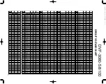
Page 21: ... 3 16 3 16 1 72 3 17 0 0 1 71 0 0 0 0 0 0 3 17 0 3 17 0 3 16 3 14 3 17 2 1 2 1 2 11 2 1 3 15 2 1 2 1 2 1 0 88 0 89 2 04 2 03 1 86 0 92 0 87 0 0 1 72 1 71 3 15 3 16 1 36 1 53 3 18 2 49 1 53 0 2 41 1 51 0 2 12 0 0 2 51 0 0 0 1 72 3 17 0 0 1 71 0 0 0 0 0 0 3 18 0 3 17 0 3 18 3 19 3 18 55 56 57 58 59 60 61 62 63 64 65 66 67 68 69 70 71 72 73 74 75 76 77 78 79 80 81 82 83 84 85 86 87 88 89 90 91 92 93 ...

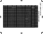
Page 22: ...2 47 0 2 52 0 2 51 0 2 2 05 0 1 96 0 42 0 42 2 51 0 8 5 16 0 1 5 19 2 2 2 2 5 24 0 0 0 0 5 24 5 24 5 16 0 0 5 24 5 2 5 24 0 0 0 2 72 5 24 5 24 3 13 24 19 26 4 28 47 26 34 26 37 30 72 26 32 28 55 I C 9 0 1 C 2 1 7 C 5 4 4 C 5 0 8 C 5 6 3 C 6 0 7 C 6 4 0 C 6 4 4 C 6 3 3 C 9 0 2 C 1 0 9 C 2 1 4 10 11 12 13 14 15 16 17 18 19 20 21 22 23 24 25 26 27 28 1 2 3 4 5 6 7 8 9 10 11 12 13 14 15 16 17 18 19 20...

Page 23: ...DVF 3080 S 8100 CAUTION For continued safety replace safety critical components only with man ufacturer s recommended parts refer to parts list indicates safety critical com ponents For continued protection against risk of fire replace only with same type and rating fuse s To reduce the risk of electric shock leakage current or resis tance measurements shall be carried out exposed parts are accept...

Page 24: ...ION IC501 DAC0 DAC1 DAC2 DAC3 DAC4 DAC5 C624 642 R666 668 R651 660 662 R661 663 664 VIDEO OPTION 24 DVF 3080 S 8100 CAUTION For continued safety replace safety criti cal components only with manufacturer s recommend ed parts refer to parts list indicates safety critical components For continued protection against risk of fire replace only with same type and rating fuse s To reduce the risk of elec...

Page 25: ...P X Y type IC502 IC501 CAUTION For continued safety replace safety critical components only with manufacturer s recom mended parts refer to parts list indicates safety critical components For continued protection against risk of fire replace only with same type and rating fuse s To reduce the risk of electric shock leakage cur rent or resistance measurements shall be carried out exposed parts are ...

Page 26: ...h a high impedance type voltmeter with no signal input The mea surement value may vary depending on the measuring instruments used or on the product 4 DRIVER CIRCUIT DIAGRAM CD DVD LD will not on KTC3875S GR T1 KTC3875S GR T1 KTC3875S GR T1 33K CAUTION For continued safety replace safety critical components only with manu facturer s recommended parts refer to parts list indicates safety critical c...

Page 27: ...r continued protection against risk of fire replace only with same type and rating fuse s To reduce the risk of electric shock leakage current or resistance measurements shall be carried out exposed parts are acceptably insulated from the supply circuit before the appliance is returned to the cus tomer The DC voltage is an actual reading measured with a high impedance type voltmeter with no signal...

Page 28: ... COMPONENT AUDIO DIGITAL S VIDEO JK601 JK6W1 601 13 J J J J J 620 608 607 609 714 748 Jx2 Jx2 J M M M 647 610 Jx2 Jx2 715 Jx2 Kx3 606 L K 712 605x2 625 626 623 M 702 613 626 10 10 627 35A 627 35A 605 605 DVF 8100 DVF 3080 E only M 711 624 604 622 622 621 YEL BLK 51 16 16 1 2 A C B Parts with exploded numbers larger than 700 are not supplied ...

Page 29: ...Desti nation Re marks H50 4932 08 BOX 3890R C177A E3 H50 4934 08 BOX 3890R C177B X3 H50 4936 08 BOX 3890R C177C E8 H50 4935 08 BOX 3890R C177E K8P8 H50 4933 08 BOX 3890R C177F Y3 H50 4931 08 BOX 3890R C177G K3P3 H10 7931 08 PACKING CASING 3920R E103A B60 5480 08 INSTRUCTION EG B60 5481 08 INSTRUCTION FR E3E8 B60 5481 08 INSTRUCTION FR P3P8 B60 5482 08 INSTRUCTION 4L E3E8 10 1C E35 3718 08 CABLE FL...

Page 30: ...na I Malaysia Y PX Far East Hawaii T England E Europe G Germany V China Shanghai Y AAFES Europe X Australia Q Russia H Korea M Other Areas indicates safety critical components Ref No Add ress New Parts Parts No Description Desti nation Re marks C546 7 CC73GCH1H221J CHIP C 220PF J C548 53 CK73GB1H104Z CHIP C 0 10UF Z C554 5 CC73GCH1H221J CHIP C 220PF J C556 9 CK73GB1H104Z CHIP C 0 10UF Z C560 CE04K...

Page 31: ... Europe G Germany V China Shanghai Y AAFES Europe X Australia Q Russia H Korea M Other Areas indicates safety critical components Ref No Add ress New Parts Parts No Description Desti nation Re marks R231 RK73GB1J102J CHIP R 1 0K J 1 16W R232 3 RK73GB1J000J CHIP R 0 J 1 16W R234 5 RK73GB1J6R8J CHIP R 6 8 J 1 16W R501 RK73GB1J103J CHIP R 10K J 1 16W R502 RK73GB1J104J CHIP R 100K J 1 16W R503 RK73FB2...

Page 32: ...S GR T1 TRANSISTOR 0TR387509AC Q603 2SC5343SG TRANSISTOR BIP 0TRAU80017A Q604 BC846ALT1 TRANSISTOR BIP 0TRON80009A Q604 KTC3875S GR T1 TRANSISTOR 0TR387509AC Q604 2SC5343SG TRANSISTOR BIP 0TRAU80017A Q605 BC846ALT1 TRANSISTOR BIP 0TRON80009A Q605 KTC3875S GR T1 TRANSISTOR 0TR387509AC Q605 2SC5343SG TRANSISTOR BIP 0TRAU80017A Q606 BC846ALT1 TRANSISTOR BIP 0TRON80009A Q606 KTC3875S GR T1 TRANSISTOR ...

Page 33: ... dBm 15 dBm Wave length 660 nm Video Section Video output format NTSC PAL Video compression DVD MPEG 2 Composite video output level 1 Vp p 75 Ω load sync negative S video output level Except for Europe Y signal 1 Vp p 75 Ω load sync negative C signal NTSC 0 286 Vp p 75 Ω PAL 0 300 Vp p 75 Ω Component Video output level Y signal 1 Vp p 75 Ω Cb signal 0 7 Vp p 75 Ω Cr signal 0 7 Vp p 75 Ω RGB output...

Reviews: