background image

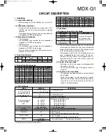
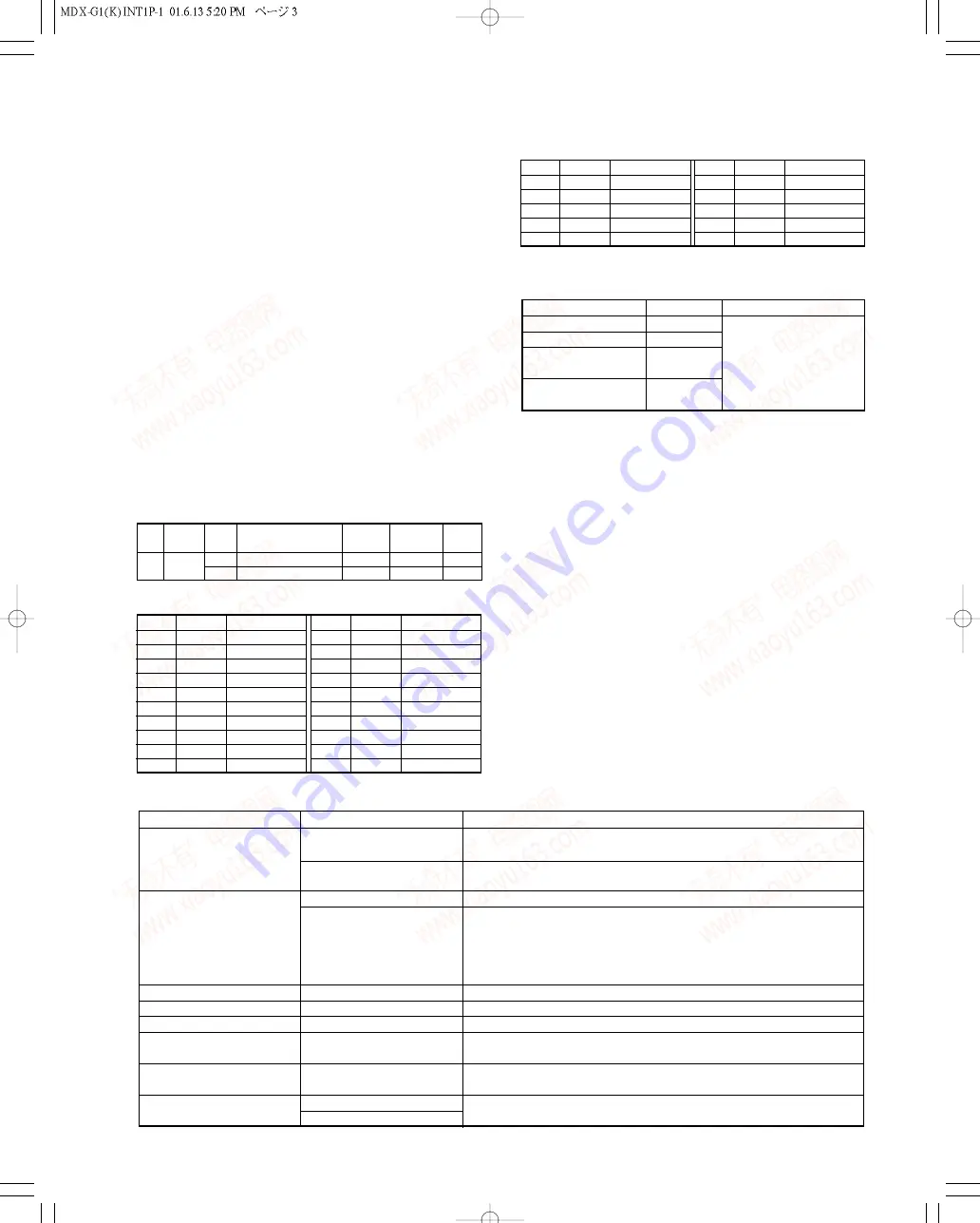
1. Initializing

1-1 Initialization Method

• While pressing the [ON/STANDBY] key, turn the AC

on.

1-2 Initialization Operation

• During the initial operation, the display shows "INI-

TIALIZE" and after that it will be retuned to standby
condition.

• If any mechanisms error occurred, the error indication

is displayed as "ERR" on the display.

1-3 Mechanism Initialization

1

CD Mechanism

• If a mechanism error occurred, the error indication is

displayed as "C ERR" on the display.

2

MD Mechanism

• If a mechanism error occurred, the error indication is

displayed as "M ERR" on the display.

• The disc will be unloaded from MD mechanism auto-

matically, if a disc is its in.

2. Tuner Destination

Set Destin- Band Receiving Frequency Channel

IF

RF

ation

Range

Space

M

E1

FM

87.5MHz~108.0MHz

50kHz

+10.7MHz 25kHz

AM

531kHz~1602kHz

9kHz

+450kHz

9kHz

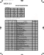
3. Tuner Preset Frequency

P.CH

Band

Frequency

1

FM

98.30MHz

2

FM

87.50MHz

3

FM

92.00MHz

4

FM

108.00MHz

5

FM

89.10MHz

6

FM

90.00MHz

7

FM

87.50MHz

8

FM

87.50MHz

9

AM

1602kHz

10

AM

999kHz

P.CH

Band

Frequency

11

AM

630kHz

12

AM

1440kHz

13

FM

106.0MHz

14

AM

531kHz

15

FM

87.50MHz

16

FM

98.00MHz

17

FM

98.50MHz

18

FM

87.50MHz

19

AM

990kHz

20

FM

97.70MHz

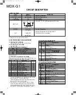
TEST MODE

KEY

SETTING

CD MODE

CD PLAY

MD MODE

MD PLAY

Insert the AC cord to

MD MECHA. ADJ.

EJECT

AC wall outlet with

MODE

pressing the left key.

SUB CLOCK OSC

MENU

DIAGNOSIS

4. Test Mode

4-1 Setting method of the Test Mode

The oscillation diagnosis(existence of oscillation and
measurement of period) of a sub clock is performed
before the test mode is entered. If the diagnosis result
is OK, the system enters the test mode.
If the diagnosis result is NG, the oscillation of the sub
clock is diagnosed again. If the result is OK, the sys-
tem enters the test mode. If the diagnosis result is
continuously NG 5 times, the system stops with
"ERR1" and "ERR2" displayed.

4-2 Cancel of the test mode

• By turning the AC off, the system is initialized and the

test mode is canceled.

• Cancel the test mode only if the power switch is

turned off

4-3 Contents of the Test Mode

• The muting during mode selection is not controlled in

the test mode.

• During the test mode, it can be operated in a special

manner that is different from an ordinary operation by
using the keys on the main body, specifically as
shown in the following tables.

KEYS

DISPLAY

OPERATION

CD-PLAY/PAUSE

05  

✽ ✽

✽ ✽

• Tracking-servo on.

(Cyclically changed

✽ 

✽ ✽

)Time Display

the mode 05 and 03

by pressing the key.)

03 --:--

• Tracking-servo off.

CD STOP

01 --:--

• Stop the CD operation.
Adjustment value/mean value

(Cyclically changed

07   FG/FE

FG value/FE value

in the stop mode

08   FB/FO

FB value/FO value

only.)

09   TG/TE

TG value/TE value

10   TB/TO

TB value/TO value

SKIP UP/SKIP DOWN

Usual Indication

• Track No up or down.

SKIP UP

Ex.Tno. 01

î

Tno. 02

• Play the first track No. in the stop mode.

SKIP DOWN

Usual Indication

• Play the last track No. in the stop mode.

*

SKIP UP

FF

• CD FF search.
• The pickup travels outward in the stop mode.

*

SKIP DOWN

FB

• CD FB search.
• The pickup travels inward in the stop mode.

MENU

HI-SPEED

• Hi speed playback 

uw

Normal speed playback 

NR-SPEED

*

Keep to press the key more than 400ms.

4-4 CD Test Mode

P.CH

Band

Frequency

21

AM

531kHz

22

FM

87.50MHz

23

FM

87.50MHz

24

FM

87.50MHz

25

FM

87.50MHz

P.CH

Band

Frequency

26

FM

87.50MHz

27

FM

87.50MHz

28

FM

87.50MHz

29

FM

108.0MHz

30

AM

945kHz

MDX-G1

3

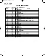
CIRCUIT DESCRIPTION

www. xiaoyu163. com

QQ 376315150

9

9

2

8

9

4

2

9

8

TEL 13942296513

9

9

2

8

9

4

2

9

8

0

5

1

5

1

3

6

7

3

Q

Q

TEL  13942296513  QQ  376315150  892498299 

TEL  13942296513  QQ  376315150  892498299 

Summary of Contents for MDX-G1

Page 1: ...SONAL STEREO SYSTEM DISC LOADING MECHANISM STANDBY TIMER ON STANDBY EJECT ONE RANDOM PGM REPEAT TRACK NO SLEEP DISC O T T PROG TOTAL O T E HIGH SPEED AUTO TUNED SP REC LP BEST HITS EX BASS MD EDIT LOUD kHz MHz AM ANTENNA PHONES AC IN AUX IN Panel ass y A60 Top ass y A52 Plastic cabinet A02 Rod antenna T90 0828 05 Miniature phone jack E11 0353 05 AC inlet E03 0374 05 Miniature phone jack E11 0399 0...

Page 2: ...ugged and plugged again while the unit is ON or due to an external cause In such a case the microcomputer should be reset as described below Unplug the power cord from the wall outlet and while holding the ON STANDBY key depressed plug the power cord again This initializes the microcomputer Note that this clears the previously stored memory CAUTION CLASS 1 LASER PRODUCT INVISIBLE LASER RADIATION W...

Page 3: ...clock is diagnosed again If the result is OK the sys tem enters the test mode If the diagnosis result is continuously NG 5 times the system stops with ERR1 and ERR2 displayed 4 2 Cancel of the test mode By turning the AC off the system is initialized and the test mode is canceled Cancel the test mode only if the power switch is turned off 4 3 Contents of the Test Mode The muting during mode select...

Page 4: ...mode is selected 1 Setting of Continuous Playback Mode No Key 1 4 Select CPLAY MODE 2 Load disc 3 MD 6 CPLAY MID c xxxx a yy error xxxx C1 error yy ADIP error CPLAY OUT c xxxx a yy error xxxx C1 error yy ADIP error 4 STOP CPLAY MODE 2 Change of Playback Points in continuous playback mode No Key Display Function Display Function 1 MD 6 2 CPLAY IN c xxxx a yy error xxxx C1 error yy ADIP error MD 6 3...

Page 5: ...onnected on the oscilloscope when two or more signals are moni tored on the oscilloscope VC and GND are short circuit ed in this case 6 4 Creating the recordable continuous recording disc This disc is used for focus bias adjustment and error rate confirmation How to create the recordable continuous recording disc is 4 6 Optical BD board pick up IC7 D3 IC1 IC2 IC6 1 Temperature compen sation offset...

Page 6: ...e waveform is difficult to be monitored con nect an oscilloscope as shown in the figure below TE1 330kΩ 10pF VC Oscilloscope 6 7 EF Balance Traverse Adjustment Connection 6 8 Automatic EF Balance Adjustment Automatic EF balance adjustment is performed TE1 VC Oscilloscope X33 ADJUSTMENT V 0 5V div H 10ms div INPUT DC mode In this case lop 82 5 mA lop mA Reading of digital voltmeter mV 1 Ω optical p...

Page 7: ...ias yyyy C1 error 4 4 Adjust yyyy to 220 5 MD 6 b xx yyyy point b 6 4 Adjust yyyy to 220 7 MD 6 C xx yyyy point c Check yyyy within 50 8 MD 6 Display shows aa bb cc xx focus bias adjust aa point a bb b cc c Notes 1 The relation between the C1 error and focus bias value is shown in the figure below Points a and b in the figure are detected by the above adjustment Focal position C is automatically o...

Page 8: ...o ground 15 X IN I Main clock input 10MHz 16 VCC BU Supply power input 5V 17 NMI Supply power input 5V 18 REM I Remote control signal input 19 NC Unused 20 BLKCK I Sub code synchronous signal input 21 CE I Chip enable input for back up detection AC On AC Off 22 NC Unused 23 MLD O CD DSP command load signal output 24 OP CL SW I Input port of detection switch for CD open close 25 MD CE I Detection p...

Page 9: ... SD detector input 83 PLL CLK O PLL IC clock output 84 PLL DATA O PLL IC data output 85 PLL CE O PLL IC chip enable output 86 PLL DO I PLL IC data input 87 90 NC Unused 91 CD PROTECT I Detection port for CD protection Protection ON Less than 4 0V 92 PROTECT I Detection port for power supply protection Protection ON Less than 0 5V 93 94 KEY2 KEY1 I A D key 1 2 input 95 TYPE I Discrimination of tune...

Page 10: ...OFTR O OFTR output 17 RFDET O RFDET output 18 GND GND 19 ENV O 3TENV output 20 VREF O VREF output 21 LD OFF O APC OFF control 22 V DET O VDET output 23 TEBPF I VDET input 24 CROSS O CROSS output 25 TEOUT O TE Amp output 26 TE I TE Amp reverse input 27 FEOUT O FE Amp output 28 FE I FE Amp reverse input 29 FBAL O F BAL control 30 TBAL O T BAL control 31 PDFR I V Amp conversion resistance adjustment ...

Page 11: ...t OPEN CLOSE SW Press the PLAY key to check that the dis play is 03 CN26 1 2 X09 ALIGNMENT POINT ALIGN FOR On the power from 0 05 to 0 15mW when the diffraction grating is correctly aligned with the RF level of 0 8Vp p or more FIG a 2 LASER CURRENT Test disc Type 4 Connect the DC voltmeter to CN25 1 and 2 in X09 B 6 Press the PLAY key to check that the dis play is 03 or 05 220mV to 550mV Note Type...

Page 12: ...1 12 10 8 9 T401 5 6 7 T402 X09 B 6 CD UNIT OPEN CLOSE DETECT J52 0044 PUSH LATCH D40 1734 5 CD MECHANISM ASS Y 5 AUX IN UNIT X09 F 6 D40 1715 MD MECHANISM ASS Y 5 MAIN UNIT X09 6500 21 A 6 DISPLAY UNIT FL X09 D 6 UNIT X09 E 6 TACT SWITCH X09 C 6 TUNER UNIT MDX G1 X33 1260 00 WIRING DIAGRAM MDX G1 12 www x i a o y u 1 6 3 c o m QQ 3 7 6 3 1 5 1 5 0 9 9 2 8 9 4 2 9 8 TEL 1 3 94 2 2 9 6 5 13 9 9 2 8...

Page 13: ...ITE RED BLACK BLUE W E FWE SLED SLED FE2 RF IOP2 VC FRDT FWDT GND RST VDD NC F TE1 FE1 SPDL SPDL TE2 VC IOP1 Q3 Q1 Q2 Q6 Q5 D3 IC3 D2 D1 IC1 IC2 IC7 IC4 IC8 IC5 IC10 D5 D6 CN3 CN1 WH1 WH2 WH3 WH2 WH3 WH1 C35 X1 C80 C2 C3 C53 L1 L4 R67 R64 R69 R35 R70 R51 R50 R52 R47 R46 R49 R48 R57 R56 R58 R45 R92 R93 R94 R88 R95 R96 R87 R76 R74 R75 R85 R31 C71 C70 C8 C5 C46 C23 C22 C38 C69 C52 C48 C58 C54 C18 R12...

Page 14: ...49 R550 R551 R556 R557 C564 R553 C567 L862 R503 C503 C502 C504 R412 R415 R414 R413 C437 C411 R402 R409 C406 R411 R423 C422 C421 R410 R417 R419 R416 R418 C417 C418 R405 D425 R403 R408 W431 W440 C420 R778 W706 W708 W704 W705 C506 W700 W518 W701 W703 R508 W482 W489 W452 W453 W709 W710 R518 W712 W483 R775 R776 W713 W853 W881 C802 R519 R771 R772 R520 R521 W883 W882 W880 W851 W852 W854 W884 POWER AMPLIF...

Page 15: ... 100 C8 0 1 33 R5 220 R6 220 40 51 50 51 50 C3 L1 100u6 3 C2 C5 0 1 28 27 R9 10K 96 92 2 2K R85 C42 470P 3 3 R70 49 48 46 47 45 78 46 45 47 49 48 R25 100 R26 100 3 5V 3 5V 3 5V 3 5V 3 5V 3 5V 3 5V B B 3 5V 3 5V B 3 5V B B 3 5V B B B B B B B B B B 0 1 C1 B B B B B 5V 5V 5V 5V B B 29 Q3 Q3 97 100 B B 83 B N C N C HVDD OUT REG NF REG VOS2 DRV REG VREG VG SEL REG GND REG VOD1 VOS1 VOD2 HGND EFM GND PD...

Page 16: ... LEVEL SHIFT MUTE LEVEL SHIFT FWD REV OPIN1 OPIN1 OPOUT1 OPIN2 OPIN2 OPOUT2 VCC VOL VOL VO2 VO2 VO1 VO1 VO4 VO4 VO3 VO3 GND BIAS MUTE OPOUT3 OPIN3 OPIN3 OPOUT4 OPIN4 OPIN4 5V 5V 23 23 S5 4 VCC FRDT 8 GND FWDT 7 6 RST 5 MODE2 2 FWE 3 NC 1 66 67 B 59 66 67 59 3 5V 3 5V 3 5V 3 5V 3 5V 5V C30 10u16 IN 1 ADJ OUT C31 R31 100u6 3 360 R30 200 2 3 3 5V 3 5V 3 5V 3 5V 3 5V 100 3 5V 3 5V CN1 Q8 Q9 Q10 MD MEC...

Page 17: ...1 100K ANT1 1 10P C2 R2 0 100 C13 8P 10K 100 R7 R8 R12 100 OSC OUT 8 7 IF OUT 68 R14 C9 0 1 C5 L4 C3 0 8P 180P C19 C7 27P L5 1000P 680 R13 560K R5 C6 4P C10 0 1 B 6 2 4P C4 IFT 680 2 2K 10K 120P C20 R9 L6 C12 0 8P C14 27P B 330P C327 C326 33K R4 1 5M B 100P C17 680K 100K 2 6P C16 18P C15 R11 3 9K R6 R10 C337 100P C336 4 7u50 C335 0 022 C334 47u25 C333 0 01 C332 10u50 10P C341 12P C340 16 5 R334 3 ...

Page 18: ... 1K R521 1 C517 R519 2 7K C759 1 3 1 2 C753 220P R763 100K 1K R761 C752 220P R762 100K 1K R760 220P 220P C750 C751 GND Lch Rch 7 5V 6 5 VCC 47K R547 83 R702 1K 84 14 24 100 1 2 24 5V R555 220 1 VCC 8 7 2 4 3 GND 6 5 5P C597 R579 2 2K 1200P C589 C591 100K C587 5600P 14 C598 5P C590 1200P C588 5600P 100K C592 2 2K R580 2 2K R578 C583 47P C584 C586 47P 100P 100P C585 R573 10K C596 100u10 R574 10K C59...

Page 19: ...1 432 1T2 or D405 406 D303 AN8806SBM IC21 Q201 204 2SC2878 B DTA124ESA MTZJ6 2 B or B30 2601 05 HSS104A or 1SS133 1SS302 or DA204U or MA143A D202 203 229 301 302 RD6 2ES B or HZS6 2N B2 D201407 408 416 418 D1 D2 Q406 2SA1577 Q R DTA114EUA or UN5111 2SC3940A R S or 2SD1768S KTA1267 Y GR or 2SA1175 F E Q401 Q404 405 Q403 Q301 S 80840ANY HD74LV1G08A LC75343M NJM4565MD HN1C01F KTC3199 Y GR or 2SC2785 ...

Page 20: ...5 203 242 224 235 202 237 823 848 216 239 822 227 817 221 241 220 236 255 229 205 244 244 218 814 846 849 219 238 238 238 DMMD 228 201 239 239 239 239 239 215 235 847 PUMD RHMD FMMD LMMD A D C C B A D B X2 X2 X2 1 2 3 A B MDX G1 26 EXPLODED VIEW MECHANISM www xiaoyu163 com QQ376315150 9 9 2 8 9 4 2 9 8 TEL 13942296513 9 9 2 8 9 4 2 9 8 0 5 1 5 1 3 6 7 3 Q Q TEL 13942296513 QQ 376315150 892498299 T...

Page 21: ...8 BLK φ3x18 F φ3x10 F φ2 6x10 φ2 6x8 φ2 6x8 φ3x8 φ3x10 BLK φ3x12 φ2 6x6 M3x10 φ3x8 N09 3481 05 N09 5188 05 N09 5324 05 N09 5326 05 N09 5354 05 N82 2608 41 N82 2608 46 N82 3008 46 N82 3010 45 N82 3012 46 N82 2606 46 N35 3010 46 N82 3008 46 708 785 620 624 660 635 640 672 652 628 642 629 785 785 745 785 636 614 613 SP1 SP1 626 638 650 651 651 612 650 766 767 644 646 641 250 26P 15P 628 637 15P 250 5...

Page 22: ...01 1E A02 3017 01 PLASTIC CABINET W 601 1E A02 3018 01 PLASTIC CABINET S 601 1E A02 3019 01 PLASTIC CABINET Y 602 1C A09 1229 08 BATTERY COVER 603 2C A29 1147 04 PANEL 604 1C A52 0926 01 TOP COVER ASSY W 604 1C A52 0938 01 TOP COVER ASSY S 604 1C A52 0941 01 TOP COVER ASSY Y 605 1C A52 0958 02 DOOR ASSY W 605 1C A52 0959 02 DOOR ASSY S 605 1C A52 0960 02 DOOR ASSY Y 606 2C A60 2044 01 PANEL ASSY W...

Page 23: ...indicates safety critical components Ref No Add ress New Parts Parts No Description Desti nation Re marks C223 CK73GB1A334K CHIP C 0 33UF K C224 CC73GCH1H100D CHIP C 10PF D C225 CC73GCH1H101J CHIP C 100PF J C226 CQ93FMG1H104J MYLAR 0 10UF J C227 CK73GB1H222K CHIP C 2200PF K C228 CQ93FMG1H223J MYLAR 0 022UF J C229 CK73GB1H472K CHIP C 4700PF K C230 CK73GB1H222K CHIP C 2200PF K C231 CQ93FMG1H102J MYL...

Page 24: ...E04RW1A101M ELECTRO 100UF 10WV C503 CE04DW0J102M ELECTRO 1000UF 6 3WV C504 CE04RW1H010M ELECTRO 1 0UF 50WV C505 CK73GB1H472K CHIP C 4700PF K C506 CC45FCH1H680J CERAMIC 68PF J C510 CE04KW1E470M ELECTRO 47UF 25WV C511 514 CE04KW1H010M ELECTRO 1 0UF 50WV C517 518 CK73GB0J105K CHIP C 1 0UF K C519 520 CE04KW1H010M ELECTRO 1 0UF 50WV C521 522 CQ93FMG1H222J MYLAR 2200PF J C523 526 CK73GB1C104K CHIP C 0 1...

Page 25: ... 0K J 1 16W R762 763 RK73GB1J104J CHIP R 100K J 1 16W R773 774 RK73GB1J271J CHIP R 270 J 1 16W R777 RK73GB1J221J CHIP R 220 J 1 16W R779 780 RK73GB1J273J CHIP R 27K J 1 16W R781 782 RK73GB1J123J CHIP R 12K J 1 16W R783 RK73GB1J111J CHIP R 110 J 1 16W R784 785 RK73GB1J221J CHIP R 220 J 1 16W R786 RS14KB3D181J FL PROOF RS 180 J 2W R801 RK73GB1J103J CHIP R 10K J 1 16W R802 RK73GB1J102J CHIP R 1 0K J ...

Page 26: ...na Shanghai Y AAFES Europe X Australia Q Russia H Korea M Other Areas indicates safety critical components Ref No Add ress New Parts Parts No Description Desti nation Re marks W271 272 R92 1252 05 CHIP R 0 OHM W516 R92 1252 05 CHIP R 0 OHM W850 R92 1252 05 CHIP R 0 OHM K401 S76 0102 05 MAGNETIC RELAY S1 16 S70 0086 05 TACT SWITCH D1 HZS6 2N B2 ZENER DIODE D1 MTZJ6 2 B ZENER DIODE D1 RD6 2ES B ZENE...

Page 27: ...J CHIP R 2 2K J 1 16W R86 RK73GB1J474J CHIP R 470K J 1 16W R87 RK73GB1J335J CHIP R 3 3M J 1 16W R88 RK73GB1J474J CHIP R 470K J 1 16W R89 RK73GB1J472J CHIP R 4 7K J 1 16W R93 RK73GB1J472J CHIP R 4 7K J 1 16W R94 RK73GB1J681J CHIP R 680 J 1 16W R95 RK73GB1J472J CHIP R 4 7K J 1 16W R96 RK73GB1J104J CHIP R 100K J 1 16W R97 R92 1853 05 CHIP RN 1 1 4W R98 R92 1854 05 RN 2 2 K 1 2W R99 RK73GB1J103J CHIP ...

Page 28: ... J 1 16W R122 123 RK73GB1J104J CHIP R 100K J 1 16W R124 126 RK73GB1J183J CHIP R 18K J 1 16W R127 128 RK73GB1J104J CHIP R 100K J 1 16W R129 RK73GB1J514J CHIP R 510K J 1 16W W2 6 R92 0679 05 CHIP R 0 OHM S1 S68 0133 05 PUSH SWITCH S2 3 S64 0052 05 LEVER SWITCH S4 S68 0132 05 PUSH SWITCH S5 S64 0052 05 LEVER SWITCH D1 2 FS1J6TP DIODE D3 4 MA111 DIODE D5 6 S1B DIODE IC1 CXD2662R MOS IC IC2 CXA2523AR I...

Page 29: ...g Singapore 349544 KENWOOD ELECTRONICS MALAYSIA SDN BHD 4 01 Level 4 Wisma Academy Lot 4A Jalan 19 1 46300 Petaling Jaya Selangor Darul Ehsan Malaysia KENWOOD ELECTRONICS THAILAND CO LTD 2019 New Pechburi Road Bangkapi Huaykwang Bangkok 10320 Thailand Amplifier section Rated output power during STEREO operation 1kHz 10 4Ω 3 5 W 3 5 W Tuner section FM tuner Tuning frequency range 87 5 MHz 108 MHz A...

Reviews: