NX-720H(G)/720H
12
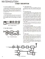
Fig. 3 Squelch Circuit
CIRCUIT DESCRIPTION
3-3. Audio amplifi er circuit
Audio processing (high-pass filter, low-pass filter, de-
emphasized and so on) in FM mode and decoding in NXDN
mode are processed by the DSP (IC502). Audio signals from
the ASIC (IC507), IC502 goes through the amplifi er (IC711).
The signal then goes through the D/A converter (IC712) and
an amplifi er (IC714).
3-4. Squelch Circuit
This circuit amplifi es the demodulated noise signal from
the ASIC (IC507) after fi ltering through a LPF and HPF cir-
cuit. The amplifi ed signal is then converted to a DC signal
by the detection circuit. The converted signal is fed back to
IC507.
ASQAPC
ASQDET
IC507
DET
IC705(1/2)
AMP
RECT
AMP
IC705(2/2)
D702
Q702
ASQ
4. Transmitter System
To TX
stage
VCO
PLL IC
IC507
IC2
IC502
DSP
LPF
IC701(1/2)
ASIC
IC703(2/2)
MIC
MIC
AMP
AGC
D703,704
Q703,704
Fig. 4 Transmitter System
4-1. Audio Band Circuit
The signal from the microphone is amplifi ed by IC703 (1/2)
and limited by the AGC circuit composed of D703, D704,
Q703 and Q704. IC703 (2/2) works as an anti-aliasing LPF
fi lter.
4-2. Base Band Circuit
The audio signal output from the Audio band circuit is
converted to digital data with a sampling frequency of 48
kHz. This digital data is sent to the DSP (IC502), and voice
signals of 300Hz or lower and frequencies of 3kHz or higher
are cut off so that an audio range 300Hz to 3kHz is extract-
ed. The audio signal is then pre-emphasized in FM mode
and synthesized with the signals, such as QT and DQT, as
required, and is then output from the ASIC (IC507). In Digital
mode, the audio signal is converted to the 4-Level FSK base
band signal and is output from IC507. The DTMF and MSK
base band signals are also generated by the DSP and out-
put from IC507.
LPF (IC701) works as smoothing fi lter. The output level
according to the transmit carrier is fi ne-adjusted according to
each modulation method.
4-3. Drive and Final amplifi er
The signal from the T/R switch (D17 is on) is amplifi ed
by the drive amplifi er (Q102 ) to 16~17dBm. The output of
the drive amplifi er is amplifi ed by the fi nal amplifi er module
(IC102) to 50W (5.0W when the power is low). The output
of the fi nal amplifi er module is then passed through the har-
monic fi lter (LPF) and antenna switch (D110, D111 are on)
and directional coupler and is applied to the antenna termi-
nal.
4-4. APC circuit
The Automatic transmission power control (APC) circuit
stabilizes the transmitter output power at a predetermined
level by detecting the power module output with the direc-
tional COUPLER and diode detector (D104 and D105). The
diode detector (D104 and D105) applies the detected volt-
age to the DC amplifi er IC103 (2/2).
The APC circuit is confi gured to protect over-current of
the power module due to fl uctuations of the load at the an-
tenna end and to stabilize transmission output at voltage and
temperature variations.
DRIVE
Q102
2SC3357-A
FINAL
IC102
RA60H1317M1-123
ANT
SW
D107,110,111
ANT
LPF
CPL
㪘㪥㪫
From T/R SW
D17
APC
For
DET
Rev
DET
D104
HSM88AS-E
D105
HSM88AS-E
IC103
NJM12
9
04RB1
Gate
bias
80T
MP
DC SW
/H_L
Q105
FK330301
Fig. 5 APC Circuit
Summary of Contents for Nexedge NX-720H
Page 83: ...NX 720H G 720H 83 MEMO ...


