background image

NX-720H(G)/720H

5

5-2. Connection procedure

1.  Connect the transceiver to the computer using the inter-

face cable.

Note:

•   You must install the KPG-46U driver in the computer to 

use the USB programming interface cable (KPG-46U).

2.  When the Power is switched on, user mode can be en-

tered immediately. When the PC sends a command, the 
transceiver enters PC mode, and “PROGRAM” is dis-
played on the LCD.


When data is transmitting from the transceiver, the red 
LED blinks.


When data is receiving by the transceiver, the green LED 
blinks.

Note:


The data stored in the computer must match the “Model 
Name” when it is written into the EEPROM.

5-3. KPG-46A description
       (PC programming interface cable: Option)

The KPG-46A is required to interface the transceiver to 

the computer. It has a circuit in its D-sub connector (KPG-46A: 
9-pin) case that converts the RS-232C logic level to the TTL 
level.

The KPG-46A connects the 8-pin microphone connector 

of the transceiver to the RS-232C serial port of the comput-
er.

5-4. KPG-46U description
        (USB programming interface cable: Option)

The KPG-46U is a cable which connects to a USB port 

on a computer.

When using the KPG-46U, install the supplied CD-ROM 

(with driver software) in the computer. The KPG-46U driver 
runs under Windows XP, Vista or 7.

The latest version of the USB driver is available for down-

load from the following URL:

 http//www.kenwood.com/usb-com/
(This URL may change without notice.)

5-5. Programming Software : KPG-141D
        (ver.3.00 or later) description

The FPU is the programming software for the transceiver 

supplied on a CD-ROM. This software runs under Windows 
XP, Vista or 7 on a PC.

The data can be input to or read from the transceiver and 

edited on the screen. The programmed or edited data can be 
printed out. It is also possible to tune the transceiver.

PC

KPG-46A or KPG-46U 
Tuning cable
(E30-3383-05)

KPG-46U

Transceiver

PC

Transceiver

PC

KPG-46A

D-SUB

(

9

-pin)

USB

FPU

Fig. 1

6. Firmware Programming Mode

6-1. Preface

Flash memory is mounted on the transceiver. This al-

lows the transceiver to be upgraded when new features are 
released in the future. (For details on how to obtain the fi  rm-
ware, contact Customer Service.)

6-2. Connection procedure

Connect the transceiver to the personal computer using 

the interface cable (KPG-46A/46U). (Connection is the same 
as in the PC Mode.)

6-3. Programming

1. Start up the fi rmware programming software (Fpro.exe(ver. 

6.1 or later)). The Fpro.exe exists in the KPG-141D in-
stalled holder.

2. Set the communications speed (normally, 115200 bps)and 

communications port in the confi  guration item.

3. Set the fi rmware to be updated by File name item.
4. Press and hold the [ ] key while turning the transceiver 

power ON. Then, the orange LED on the transceiver 
lights and “FIRM PRG” is displayed.

5. Check the connection between the transceiver and the 

personal computer, and make sure that the transceiver is 
in the Program mode.

6. Press “write” button in the window. When the transceiver-

starts to receive data, the "LOADING" display lights.

7. If writing ends successfully, the checksum is calculated 

and a result is displayed.

8. If you want to continue programming other transceivers, 

repeat steps 4 to 7.

REALIGNMENT

Summary of Contents for Nexedge NX-720H

Page 1: ... Modular jack E58 0535 05 CONTENTS GENERAL 2 SYSTEM SET UP 4 REALIGNMENT 4 INSTALLATION 7 DISASSEMBLY FOR REPAIR 9 CIRCUIT DESCRIPTION 11 COMPONENTS DESCRIPTION 17 PARTS LIST 19 EXPLODED VIEW 29 PACKING 30 TROUBLE SHOOTING 31 ADJUSTMENT 35 TERMINAL FUNCTION 56 PC BOARD DISPLAY UNIT X54 3830 10 60 TX RX UNIT X57 8230 1X 62 INTERCONNECTION DIAGRAM 66 SCHEMATIC DIAGRAM 67 BLOCK DIAGRAM 78 LEVEL DIAGR...

Page 2: ...deviation and power output should be checked as should receiver sensitivity squelch operation and audio output Signalling equipment operation should be verified 3 PLANNING THE INSTALLATION 3 1 General Inspect the vehicle and determine how and where the ra dio antenna and accessories will be mounted Plan cable runs for protection against pinching or crush ing wiring and radio installation to preven...

Page 3: ...ended be sure the additional wire is sufficient for the current to be carried and length of the added lead 4 INSTALLATION PLANNING CONTROL STATIONS 4 1 Antenna system Control station The antenna system selection depends on many factors and is beyond the scope of this manual Your KENWOOD dealer can help you select an antenna sys tem that will best serve your particular needs 4 2 Radio location Sele...

Page 4: ...r and PC Data programming mode Used to read and write frequency data and other features to and from the transceiver PC test mode Used to check the transceiver using the PC This feature is included in the FPU PC tuning mode Used to tune the transceiver using the PC Firmware programming mode Used when changing the main program of the flash memory Clone mode Used to transfer programming data from one...

Page 5: ... The FPU is the programming software for the transceiver supplied on a CD ROM This software runs under Windows XP Vista or 7 on a PC The data can be input to or read from the transceiver and edited on the screen The programmed or edited data can be printed out It is also possible to tune the transceiver PC KPG 46A or KPG 46U Tuning cable E30 3383 05 KPG 46U Transceiver PC Transceiver PC KPG 46A D ...

Page 6: ...s END and the source red LED turned off and the target automatically operates in the User mode The target can then be operated by the same pro gram as the source 5 The other target can be continuously cloned Carry out the operation in step 2 to 4 7 1 Adding the data password If the read authorization password is set in the optional feature menu you must enter the password Source trans ceiver to ac...

Page 7: ... use the HR1 The voltage range is from 5V to 16V 13 HR1 14 HR2 3 GND Default Note You must set up using the KPG 141D 13 14 Horn alert cable Square plug Crimp terminal 13 14 15 10 11 12 7 8 9 4 5 6 1 2 3 KCT 60 3 Ignition Sense Cable KCT 18 Option The KCT 18 is an optional cable for enabling the ignition function The ignition function lets you turn the transceiver power on and off with the car igni...

Page 8: ...o RS 232C level FNC1 TXD 6pin FNC2 RXD 7pin FNC3 RTS 8pin and FNC4 CTS 9pin of D SUB 15 pin connector are con figured at the TTL level as the default value But you can change these serial port level to RS 232C level through the RS 232C level converter IC IC516 by configuring the port Remove the R664 R635 R662 R659 R658 and R632 chip jumpers and solder the chip jumpers to R666 R633 R665 R663 R660 a...

Page 9: ...nnector of the panel as sembly Flat cable 4 Hook the finger to hole and while pulling the speaker holder to this side expand the panel side of a to c and remove the speaker holder from the front panel Speaker holder a b c 5 When removing the TX RX PCB first remove the top packing Then remove the solder of the antenna hot pin and posi tive terminal of the DC cord Remove the 16 screws from the TX RX...

Page 10: ...Reassembly 1 The tab from a to c is applied the front panel first And d to f tabs inside the front panel is pushed Display PCB Speaker holder a b c d e f 2 When mounting the panel assembly pass the flat cable through the hole of the chassis as shown below then con nect the flat cable to connector of the panel assembly Panel assembly Panel assembly Chassis Chassis Hole of the chassis 3 Fit the pane...

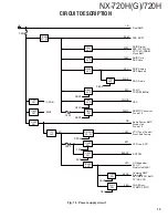
Page 11: ...or The input voltage to the variable capacitor is regulated by the voltage output from the D A converter IC712 The signal is amplified by an RF am plifier Q202 and passed through the bandpass filter L207 209 210 and 220 The resulting signal is applied to the first mixer Q201 where it is mixed with the first local oscillator signal output from the frequency synthesizer to produce the first IF 49 95...

Page 12: ...and synthesized with the signals such as QT and DQT as required and is then output from the ASIC IC507 In Digital mode the audio signal is converted to the 4 Level FSK base band signal and is output from IC507 The DTMF and MSK base band signals are also generated by the DSP and out put from IC507 LPF IC701 works as smoothing filter The output level according to the transmit carrier is fine adjuste...

Page 13: ... to the VCO CV terminal and realizes the Phase Locked Loop for the return control This allows the VCO oscillation frequency to accurately match lock the desired frequency When the frequency is controlled by the PLL the fre quency convergence time increases as the frequency dif ference increases when the set frequency is changed To supplement this the ASIC IC507 is used before control by the PLL IC...

Page 14: ... IC1 the information is passed to IC507 through the serial line 6 5 DSP The DSP circuit consists of a DSP IC502 and processes the base band signal The DSP operates on an external clock of 18 432MHz the same as the IC507 the I O section operates at 3 3V and the core section operates at 1 5V The DSP carries out the following processes 4 level FSK processing Analog FM pre emphasis de emphasis Vocoder...

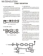
Page 15: ... 㪪㪮 㪨㪋㪇㪋 㪛㪛㪚㪣㪢 㪪㪮 㪨㪋㪇㪉 㪫㪯㪚 㪛㪪㪮 㪘㪭㪩 㪠㪚㪋㪇㪋 㪆㪦㪭㪩㪙 㪈㪌㪇㪚 㪏㪇㪫 㪏㪇㪘㪥㪫 㪌㪇㪚 㪌㪇㪚㪪 㪌㪇㪩 㪪㪮 㪨㪋㪇㪏 㪪㪮 㪨㪋㪈㪎 㪪㪘㪭㪜 㪩㪯㪚 㪏㪇㪚 㪝㪥㪚㩷㪙㪬㪝㪝 㪘㪪㪠㪚㩷㪛㫀㪾㫀㫋㪸㫃 㪛㪪㪧㩷㪠㪆㪦㪃㩷㪝㪣㪘㪪㪟 㪭㪚㪫㪚㪯㪦㪃㩷㪪㪩㪘㪤 㪚㫃㫆㪺㫂㩷㪙㫌㪽㪽 㪘㪪㪠㪚㩷㪚㫆㫉㪼 㪛㪪㪧㩷㪚㫆㫉㪼 㪘㪪㪠㪚㩷㪘㫅㪸㫃㫆㪾 㪞㪧㪪㩷㪙㪸㪺㫂㩷㫌㫇 㪛㪘㪚㪃㩷㪘㫌㪻㫀㫆 㪧㪣㪣㩷㪠㪚 㪫㪚㪯㪦㩿㪈㪍㪅㪏㪤㪟㫑㪀 㪞㪧㪪 㪩㪪㪉㪊㪉㪚㩷㪚㫆㫅㫍㪼㫉㫋㪼㫉 㪛㪄㫊㫌㪹㩷㪈㪌 㪘㫌㪻㫀㫆㩷㪧㫆㫎㪼㫉㩷㪘㪤㪧 㪛㫀㫊㫇㫃㫐㩷㪬㫅㫀㫋 㪛㪄㫊㫌㪹㩷㪈㪌 㪭㪚㪦㩷㪫㫌㫅㪼㩷㩿㪘㫊㫊㫀㫊㫋㪀 㪝㫉㫆㫅㫋㩷㪜㫅㪻㩷㪫㫌㫅㫀㫅㪾 㪫㪯㩷㪛㫉㫀㫍㪼㪃㩷㪘㪧㪚 㪘㪥㪫㩷㪪㪮 㪠㪆㪦㩷㪜㫏㫇㪸㫅㪻㪼㫉 㪧㪣㪣㩷㪠㪚 㪛㫀㫊㫇㫃㫐㩷㪬㫅㫀㫋㩿㪣㪜㪛㪀 ...

Page 16: ...the FM detection signal sent to the DSP circuit and the resulting signal is decoded by the DSP 9 Compander Circuit The term compander means compressor and expander The compander reduces noise by utilizing a compressor and an expander The DSP IC502 performs this operation The ompander can be turned on or off using the FPU 10 GPS Circuit GPS model only The GPS information function can be used by set...

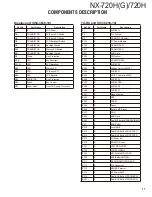
Page 17: ...ower Module IC103 IC OP AMP APC IC201 IC DC AMP BPF IC301 IC AND Gate IC303 IC FM System IC304 IC DC AMP RSSI IC401 IC AVR 33M IC402 IC Voltage Detector BINT IC404 IC AVR 50C IC405 IC DC DC Converter 50M IC406 IC AVR 33A IC407 IC AVR 33GPS IC408 IC AVR 15M IC409 IC AVR 33C IC501 IC Flash Memory IC502 IC DSP IC503 IC SRAM IC504 IC Reset IC506 IC Buffer AMP Clock IC507 IC ASIC IC508 IC AND Gate IC50...

Page 18: ...otection D4 Variable Capaci tance Diode RX VCO Frequency Control D5 Variable Capaci tance Diode TX VCO Frequency Control D6 Variable Capaci tance Diode PLL f in BPF Tune D7 Variable Capaci tance Diode RX VCO Assist Tune D8 Variable Capaci tance Diode TX VCO Assist Tune D9 10 Variable Capaci tance Diode RX VCO Assist Tune D11 Variable Capaci tance Diode TX VCO Assist Tune D13 Variable Capaci tance ...

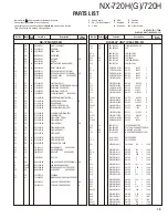
Page 19: ...2A331J CHIP R 330 J 1 10W R19 RK73GB2A221J CHIP R 220 J 1 10W R20 RK73HB1J000J CHIP R 0 J 1 16W R22 RK73HB1J000J CHIP R 0 J 1 16W R23 RK73HB1J473J CHIP R 47K J 1 16W R24 25 RK73HB1J332J CHIP R 3 3K J 1 16W R26 RK73HB1J472J CHIP R 4 7K J 1 16W R28 RK73FB2B121J CHIP R 120 J 1 8W R29 RK73FB2B221J CHIP R 220 J 1 8W R34 37 RK73GB2A271J CHIP R 270 J 1 10W R38 40 RK73HB1J472J CHIP R 4 7K J 1 16W 1 1B A02...

Page 20: ...5 CK73HB1H471K CHIP C 470PF K C156 CC73HCH1H101J CHIP C 100PF J C157 CK73HB1H102K CHIP C 1000PF K C158 CK73HB1H471K CHIP C 470PF K C161 CC73GCH1H040C CHIP C 4 0PF C C163 CC73GCH1H220J CHIP C 22PF J C165 CK73HB1H471K CHIP C 470PF K R41 RK73HB1J101J CHIP R 100 J 1 16W R42 RK73HB1J272J CHIP R 2 7K J 1 16W R43 RK73HB1J103J CHIP R 10K J 1 16W R44 RK73HB1J222J CHIP R 2 2K J 1 16W R45 RK73HB1J472J CHIP R...

Page 21: ...5K CHIP C 2 2UF K C436 CK73HB1H103K CHIP C 0 010UF K C437 CK73FB1E475K CHIP C 4 7UF K C438 439 CK73GB1H104K CHIP C 0 10UF K C440 C92 0875 05 ELECTRO 47UF 25WV C441 CK73GB1C225K CHIP C 2 2UF K C167 CC73GCH1H150J CHIP C 15PF J C168 CK73HB1H471K CHIP C 470PF K C171 CC73HCH1H101J CHIP C 100PF J C172 173 CK73HB1H471K CHIP C 470PF K C175 CC73FCH1H390J CHIP C 39PF J C176 C93 0564 05 CHIP C 22PF J C177 17...

Page 22: ...F K C735 CK73GB0J106K CHIP C 10UF K C738 CK73HB1A104K CHIP C 0 10UF K C739 CK73HB1A105K CHIP C 1 0UF K C740 CK73HB1H102K CHIP C 1000PF K C741 CK73HB1A224K CHIP C 0 22UF K C442 CK73HB1H103K CHIP C 0 010UF K C443 CK73GB1E105K CHIP C 1 0UF K C445 446 CK73HB1H103K CHIP C 0 010UF K C447 CK73GB1E105K CHIP C 1 0UF K C448 CK73HB1H103K CHIP C 0 010UF K C449 CK73GB1E105K CHIP C 1 0UF K C450 451 CK73FB1A106K...

Page 23: ...H L215 216 L41 3378 14 SMALL FIXED INDUCTOR 33NH L220 L40 2785 92 SMALL FIXED INDUCTOR 270NH L221 L40 5663 71 SMALL FIXED INDUCTOR 5 6NH L232 233 L41 3978 14 SMALL FIXED INDUCTOR 39NH L301 L41 1585 14 SMALL FIXED INDUCTOR 150N L302 L40 5681 86 SMALL FIXED INDUCTOR 0 56UH C743 CC73HCH1H470J CHIP C 47PF J C744 CK73HB1A224K CHIP C 0 22UF K C746 CK73HB1A104K CHIP C 0 10UF K C747 CC73HCH1H221J CHIP C 2...

Page 24: ...R145 RK73GB2A000J CHIP R 0 J 1 10W R146 RK73HB1J393J CHIP R 39K J 1 16W R147 RK73HB1J124J CHIP R 120K J 1 16W R148 RK73HB1J000J CHIP R 0 J 1 16W R149 RK73HB1J103J CHIP R 10K J 1 16W L304 L40 5675 92 SMALL FIXED INDUCTOR 56NH L307 L40 2291 86 SMALL FIXED INDUCTOR 2 2UH L309 L40 1085 57 SMALL FIXED INDUCTOR 100NH L310 L92 0138 05 CHIP FERRITE L317 L41 3985 39 SMALL FIXED INDUCTOR 0 39UH L319 L41 188...

Page 25: ...R519 RK73HB1J000J CHIP R 0 J 1 16W R521 522 RK73HB1J104J CHIP R 100K J 1 16W R524 RK73HB1J000J CHIP R 0 J 1 16W R525 RK73HB1J474J CHIP R 470K J 1 16W R526 RK73HB1J104J CHIP R 100K J 1 16W R150 RK73HB1J124J CHIP R 120K J 1 16W R152 RK73HB1J102J CHIP R 1 0K J 1 16W R154 RK73HB1J000J CHIP R 0 J 1 16W R155 RK73HB1J223J CHIP R 22K J 1 16W R157 158 RK73HB1J333J CHIP R 33K J 1 16W R159 160 RK73HB1J000J C...

Page 26: ...K73GB2A000J CHIP R 0 J 1 10W R800 RK73HB1J104J CHIP R 100K J 1 16W R801 RK73HB1J102J CHIP R 1 0K J 1 16W H R801 802 RK73HB1J102J CHIP R 1 0K J 1 16W HG R803 804 RK73HB1J472J CHIP R 4 7K J 1 16W R531 RK73HB1J104J CHIP R 100K J 1 16W R532 RK73HB1J000J CHIP R 0 J 1 16W R533 534 RK73HB1J473J CHIP R 47K J 1 16W R536 RK73HB1J000J CHIP R 0 J 1 16W R541 RK73HB1J101J CHIP R 100 J 1 16W R546 RK73HB1J000J CH...

Page 27: ...Q201 3SK318 FET Q202 NESG240034 TRANSISTOR Q303 2SC5108 Y F TRANSISTOR Q305 2SC4215 F Y TRANSISTOR R805 806 RK73HB1J102J CHIP R 1 0K J 1 16W R810 RK73HB1J123J CHIP R 12K J 1 16W R811 RK73HB1J103J CHIP R 10K J 1 16W R813 RK73HB1J102J CHIP R 1 0K J 1 16W R814 RK73HB1J391J CHIP R 390 J 1 16W R816 RK73HB1J123J CHIP R 12K J 1 16W R818 RK73HB1J332J CHIP R 3 3K J 1 16W R819 820 RK73HB1J222J CHIP R 2 2K J...

Page 28: ...OR Q414 EMD9 TRANSISTOR Q415 2SC4738 GR F TRANSISTOR Q416 2SA1832 GR F TRANSISTOR Q417 EMD5 TRANSISTOR Q418 LTC014EEBFS8 TRANSISTOR Q501 FK330301 FET Q502 LTC014TEBFS8 TRANSISTOR Q503 MTM981400BF FET Q504 LTC014TEBFS8 TRANSISTOR Q701 FK330301 FET Q702 KTC4075E Y GR TRANSISTOR Q703 2SA1832 GR F TRANSISTOR Q704 2SC4738 GR F TRANSISTOR Q705 706 SSM3J15FS FET Q708 LTC014EEBFS8 TRANSISTOR Q709 SSM6N37F...

Page 29: ...ts must be ordered separately 3 2 1 B A 1 B B B 701 Caution label 702 Model name plate C C X57 X57 X57 TX RX unit Display unit B Cx13 31 J501 IC102 R358 13 10 2 3 33 51 32 46 23 7 20 48 101 5 26 IC714 14 J701 X54 102 X54 D23 X54 J1 X54 D22 X54 103 X54 104 X54 A N30 2605 48 M2 6x5 B N67 3008 48 C N87 2608 48 2 6X8 15 16 24 19 25 17 22 A A 28 6 27 H type or 21 11 704 703 Cx2 Cx2 HG type 9 M3x8 EXPLO...

Page 30: ...12 DC cord assy E30 7523 55 18 Fuse Blade type x 2 F52 0024 05 705 Protection bag 50 Screw set N99 2039 05 43 Holder MIC J19 1584 15 52 Microphone KMC 35 T91 0639 55 706 Pamphlet 8 Instruction Manual B62 2421 00 41 Packing Fixture H12 4346 12 Parts with the exploded numbers larger than 700 are not supplied PACKING ...

Page 31: ...f the voltage becomes normal the SRAM is broken 15M has an abnormal voltage ASIC Remove L510 to check the voltage of the 15M If the voltage becomes normal the ASIC is broken DSP Remove R505 to check the voltage of the 15M If the voltage becomes normal the DSP is broken 33A has an abnormal voltage ASIC Remove R571 to check the voltage of the 33A If the voltage becomes normal the ASIC is broken If t...

Page 32: ...and 50C is abnormal the BGA parts are not broken Remove R407 If the ASIC side is 0V the ASIC FALSH SRAM may be broken s Panel control Disply unit Checking the Control signal Points to be checked Normal voltage LCDCE CN514 20 pin 5 0V or 0V LCDCL CN514 21 pin LCDDI CN514 19 pin If Disply unit is removed and a waveform becomes normal the BGA parts are not broken When a waveform is abnormal the IC511...

Page 33: ...KRA 40 The GPS power supply circuit may be broken Check IC407 and its surrounding parys The backup power supply is faulty Check IC 406 33A The output of the GPS data is verified IC801 5pin Square wave form The RXD circuit is fauity Replace D512 The signal line parts are faulty Verify each part Connect the KRA 40 correctly Verify the TXD data output from the GPS module CN802 Square wave form Verify...

Page 34: ...Using the KPG 141D select your desired item Model Name and Frequency from the Model Product Information menu then use Program Write Data to the Transceiver to write the FPU data PC Programming mode When writing to the transceiver a Warning Message corresponding to the item selected appears Click OK to continue writing the data 3 Enter Program Test Mode then adjust the various adjustment data PC Te...

Page 35: ...Controls Power switch Modular MIC jack Programmable function keys Volume Up Down key Channel Up Down key LCD KMC 36 OPTION Keypad PTT Key operation Key not appears on the LCD display Function Display Test channel up down Channel No Push Squelch level up Hold Squelch off Squelch level Squelch off icon appears Wide Narrow Very narrow Wide W Narrow N Very narrow V Shift to panel tuning mode Function ...

Page 36: ...to obtain the frequencies you want in actual operation Analog mode signaling No RX TX 1 None None 2 None 100Hz Square Wave 3 LTR Data AREA 0 GOTO 12 HOME 12 ID 47 FREE 25 LTR Data AREA 0 GOTO 12 HOME 12 ID 47 FREE 25 4 QT 67 0Hz QT 67 0Hz 5 QT 151 4Hz QT 151 4Hz 6 QT 210 7Hz QT 210 7Hz 7 QT 254 1Hz QT 254 1Hz 8 DQT D023N DQT D023N 9 DQT D754I DQT D754I 10 DTMF 159D DTMF 159D 11 None DTMF Code 9 12...

Page 37: ...nter High High Narrow Wide Very narrow Narrow Very narrow Wide Key operation Key Function Push Hold 1 second Adjustment value up down 20Hz 2kHz During transmis sion in balance adjustment Wide Narrow Very narrow Shift to panel test mode To enter 5 reference level adjustments Writes the adjustment value Go to next adjustment item Back to last adjust ment item Volume level up down PTT Transmit 0 to 9...

Page 38: ...NXDN Narrow Very Narrow Maximum Deviation of NXDN Narrow Very Narrow is adjusted Maximum Deviation Analog Wide Narrow Maximum Deviation of Analog Wide Narrow is adjusted This item must be adjusted before all adjustment items for tone deviations are adjusted Note Maximum Deviation Analog Narrow must be adjusted before CW ID Deviation NXDN Very Narrow is adjusted QT Deviation QT tone deviation is ad...

Page 39: ...Transmitter Section 2 1 1024 8 Mid Transmit Power 5 Transmitter Section 2 1 1024 9 Low Transmit Power 5 Transmitter Section 2 1 1024 10 Balance 5 Transmitter Section 2 1 1024 11 Maximum Deviation NXDN 5 5 Transmitter Section 4 1 1024 12 Maximum Deviation Analog 5 5 Transmitter Section 5 1 1024 13 QT Deviation 1 1 Transmitter Section 6 1 1024 14 DQT Deviation 1 1 Transmitter Section 7 1 1024 15 LTR...

Page 40: ... Center High H High H Mid Trancemit Power MPWR High Trancemit Power HPWR Low Trancemit Power LPWR Mid Trancemit Power Limit MLMT High Trancemit Power Limit HLMT Low Trancemit Power Limit LLMT Balance BAL NXDN Deviation NDEV Narrow Narrow Narrow Narrow Narrow Narrow Narrow Narrow NXDN Deviation NDEV Very Narrow Panel test mode For all adjustment items press the key to write the adjustment value N W...

Page 41: ...SS Very Narrow Narrow RSSI High HRSS Narrow Squelch Tight SQLT 5 reference level Adjustments 5 reference level Adjustments 5 reference level Adjustments 5 reference level Adjustments 5 reference level Adjustments 5 reference level Adjustments Analog MAX Deviation ADEV Wide Wide Wide Wide Wide Wide Wide Wide Wide Wide Wide QT Deviation QT DQT Deviation DQT DTMF Deviation DTMF MSK Deviation MSK Sing...

Page 42: ... more 8 AF Volt Meter AF VM Frequency Range 50Hz to 10kHz Voltage Range 1mV to 10V 9 Audio Generator AG Frequency Range 50Hz to 5kHz or more Output 0 to 1V 10 Distortion Meter Capability 3 or less at 1kHz Input Level 50mV to 10Vrms 11 4 Dummy Load Approx 4 10W 12 Regulated Power Supply 13 6V approx 20A adiustable from 9V to 17V Useful if ammeter equipped 13 Spectrum Analyzer Frequency Range 40MHz ...

Page 43: ...nnel Channel 2 Test Signaling Mode Analog Signaling 1 PTT Press Transmit button 3 CH Sig 3 1 PTT ON 3 Test Channel Channel 3 Test Signaling Mode Analog Signaling 1 PTT Press Transmit button 3 Low power check 1 CH Sig 1 1 PTT ON 1 Test Channel Channel 1 Test Signaling Mode Analog Signaling 1 PTT Press Transmit button 3 5W 6 5W 7A or less 2 CH Sig 2 1 PTT ON 2 Test Channel Channel 2 Test Signaling M...

Page 44: ...y PC test mode 1 Adj item Receive Assist 2 Adj item Low1 Low2 Low3 Center1 Center2 Center3 High1 High2 Hi gh3 Press Apply All button to store the adjustment value PC test mode PC test mode Automatic Adjustment Press Tune Assist Voltage button Press Apply All but ton to store the adjust ment value after the automatic adjustment has finished Manual Adjustment V indicator on the PC window shows VCO l...

Page 45: ...ing conditions Temperature range of 20 C to 26 C 68 0 F to 78 8 F The temperature is displayed on the Frequency adjust ment screen of the KPG 141D and the LCD of the trans ceiver Use an accuracy of 0 003ppm for the SSG Use a standard oscillator if necessary SSG ANT PC test mode Press Start button of Auto Tuning Press Apply button to store the adjustment value after the automatic ad justment was fi...

Page 46: ...un ing mode PC test mode 53 0W 2 0W PC test mode Press Apply All button to store the adjustment value after all adjust ment point was adjusted Mid Transmit power Limit 1 Adj item MLMT Adjust 2 Adj item M LMT_ M L MT_ M L M T_ M L M T _ M L M T _ 3 PTT ON 4 Press key to store the adjust ment value 1 TEST CH Low Low Center High High 5 point 2 Transmit Press Apply All button to store the adjustment v...

Page 47: ...was adjusted Low Transmit power 1 Adj item LPWR Adjust 2 Adj item L PWR_ L P WR_ L P W R_ L P W R _ L P W R _ 3 PTT ON 4 Press key to store the adjust ment value 1 TEST CH Low Low Center High High 5 point 2 Transmit Press Apply All button to store the adjustment value 5 0W 0 2W 7 0A or less PC test mode Press Apply All button to store the adjustment value after all adjust ment point was adjusted 3...

Page 48: ...deviation is between 2995Hz and 3117Hz Deviation meter LPF 3kHz HPF OFF Panel tuning mode PTT ON PC test mode PTT Press Trans mit button 2995 3117Hz PC test mode Press Apply All button to store the adjustment value after all adjust ment point was adjusted Very Narrow Adj item NDEV Adjust PTT ON Press key to store the adjustment value 1 Adj item Maximum Deviation NXDN Very Narrow PTT Press Transmit...

Page 49: ...alue 1 Adj item Maximum Deviation Analog Wide PTT Press Transmit button Press Apply All but ton to store the adjust ment value Write fixed value 513 for each adjustment point Transmit at each adjustment point and check that the Analog deviation is between 4150Hz and 4250Hz Deviation meter LPF 15kHz HPF OFF Panel tuning mode PTT ON PC test mode PTT Press Transmit button 4150 4250Hz PC test mode Pre...

Page 50: ...tem LTR Deviation Analog Narrow Deviation meter LPF 3kHz HPF OFF PTT Press Transmit button Press Apply button to store the adjustment value Deviation meter Oscillo scope ANT Panel tun ing mode PC test mode Write the value 465 Reference value 0 75kHz 0 05kHz Wide 1 Adj item LTR Adjust PTT ON Press key to store the adjustment value 1 Adj item LTR Deviation Analog Wide PTT Press Transmit button Press...

Page 51: ...n adjust Narrow 1 Adj item MSK Adjust Deviation meter LPF 15kHz HPF OFF PTT ON Press key to store the adjust ment value 1 Adj item MSK Deviation Analog Narrow Deviation meter LPF 15kHz HPF OFF PTT Press Trans mit button Press Apply button to store the adjustment value Deviation meter Oscillo scope ANT Panel tun ing mode PC test mode Write the value 513 Reference value 1 50kHz 0 05kHz Wide 1 Adj it...

Page 52: ...adjust 2 Maximum Deviation adjust Wide 3 DQT Deviation adjust Wide 1 Balance adjust 2 Maximum Deviation adjust Narrow 3 DQT Deviation adjust Narrow LTR 1 Balance adjust 2 Maximum Deviation adjust Wide 3 LTR Deviation adjust Wide 1 Balance adjust 2 Maximum Deviation adjust Narrow 3 LTR Deviation adjust Narrow DTMF 1 Balance adjust 2 Maximum Deviation adjust Wide 3 DTMF Deviation adjust Wide 1 Balan...

Page 53: ...et H SENS1 High 122 Preset H SENS1 High 152 Preset VHF Increase the adjustment value from the preset value to get 12dB SINAD SSG output 119dBm 0 25uV Mod 1kHz 1 5kHz Note The preset value of Sensitivity 2 must be written before adjusting Sensitivity 1 3 ensitivity2 adjust This adjustment can be performed only PC test mode 1 Adj item Sensitivity 2 2 Adj item Low Low Center High High Press Apply All...

Page 54: ...ore the adjustment value 6 Low RSSI at 118dBm adjust 1 Adj item LRSS Adjust 2 Adj item L RSS L R SS L R S S L R S S L R S S _ SSG output 118dBm 0 28uV MOD 1kHz 1 5kHz 1 Adj item Low RSSI Analog Narrow 2 Adj item Low Low Center High High SSG output 118dBm 0 28µV MOD 1kHz 1 5kHz SSG ANT Ext SP connector PC test mode Panel tuning mode After input signal from SSG press B key to store the adjustment va...

Page 55: ...t Squelch Analog Narrow 2 Adj item Low Low Center High High Press Apply All button to store the adjustment value SSG ANT Ext SP connector PC test mode Write the value as VHF Analog Narrow S QLT 248 S Q LT 248 S Q L T 248 S Q L T 248 S Q L T _ 248 Analog Wide S QLT 255 S Q LT 255 S Q L T 255 S Q L T 255 S Q L T _ 255 Analog Wide 1 Adj item Tight Squelch Analog Wide 2 Adj item Low Low Center High Hi...

Page 56: ... MIC jack 1 MBL O MIC backlight control 2 SB O Battery voltage DC supply 3 GND Ground 4 PTT I O PTT PC serial data from radio 5 ME MIC ground 6 MIC I MIC signal input 7 HOOK I HOOK PC serial data to radio 8 DM I O MIC data detection TX RX unit X57 8230 10 Pin No Name I O Function CN514 to Disply unit CN1 1 SB O Battery voltage DC supply 2 SB O Battery voltage DC supply 3 SP O Speaker output 4 SP O...

Page 57: ...Micro phone 6 MIC I Analog Audio input Aoutput 5 mVrms Copling Capacitor 10 uF Input impednce 600 Allowable Frequency 300 3000 Hz 7 HOOK RXD I Digital Digital transistor input Pull Up 5 0V 4 7k VIH 2 7 5 2 V VIL 0 3 0 9 V Baud rate 115200 bps 8 DM I Digital CMOS input Pull Up 5 0V 47k VIH 2 7 5 2 V VIL 0 3 0 5 V VOH 3 7 5 2 V O Digital VOL 1 1 V 15pin D sub Connector Specification Pin No Pin Name ...

Page 58: ...Digital RS 232C Serial port TXD Voltage Swing 5 9 V 3k Load Baud Rate 19200 bps CL 100 pF 7 FNC2 RXD I O Digital Programmable I O VIH 4 0 5 2 V VIL 0 5 1 0 V VOH Io 1 5mA 4 0 5 2 V VOL Io 1 5mA 1 1 V RXD RS 232C I Digital RS 232C Serial port RXD Input Voltage Range 30 30 V Threshold Low 0 5 1 3 V Threshold High 1 75 2 6 V 8 FNC3 I O Digital Programmable I O VIH 4 0 5 2 V VIL 0 5 1 0 V VOH Io 1 5mA...

Page 59: ...wer 5V DC Power supply Output Voltage 4 5 5 0 5 25 V Output Current 100 mA 13 HR1 I Analog Horn alert signal input Input Voltage 5 16 V Input Current 2 0 A Rds ON 55 108 m TXD2 TTL O Digital VOH Io 1 5mA 4 0 5 2 V VOL Io 1 5mA 1 1 V 14 HR2 O Analog Horn alert signal output Output Voltage 16 V Output Current 2 0 A RXD2 TTL or RS 232C I Digital Input Range 30 30 V Threshold Low 0 6 V Threshold High ...

Page 60: ...R1 R35 R36 R37 R38 R39 R5 R7 R9 R40 R41 R42 R43 R44 R45 CN1 C10 C11 C12 C13 C14 C15 1 3 6 4 SB SP SP BLC MBL RLED GLED BLED GND GND GND GND GND GND EMG 50C LCDDI LCDDO LCDCE LCDCL MIC ME HOOK POWER MKEY PTT NX 720H G 720H PC BOARD SB SP SP DISPLAY UNIT X54 3830 10 Component side view J79 0345 09 DISPLAY UNIT X54 3830 10 Foil side view J79 0345 09 D5 D8 J1 D11 D14 D15 D18 D19 D22 D23 D24 NC ...

Page 61: ...SPLAY UNIT X54 3830 10 Foil side view J79 0345 09 D6 D7 D9 D12 D13 D16 D17 D19 D20 D21 D24 Ref No Address IC1 Q3 Q6 Q8 Q9 Q10 Q11 D1 D2 D25 D26 D27 12K 11B 12B 11F 11E 12B 11F 10B 9C 10B 12M 11E Component side Foil side Layer 1 Layer 2 Component side Foil side Layer 1 Layer 2 Ref No Address D5 D7 D8 D9 D11 D12 D13 D14 D15 D17 D16 D18 D19 D21 D20 D22 D23 4D 7K 7G 7O 3G 3N 4N 4G 3H 4M 3M 4H 3J 4K 3K...

Page 62: ... R628 R813 R810 R613 R614 R617 R610 R615 R814 R627 C765 R730 R728 R724 C732 C708 C729 C719 C702 C705 C716 C707 C706 C701 C720 C728 C770 C725 C709 C722 C752 C753 R743 C738 R742 C740 R741 C739 C741 R838 R181 R128 R837 R801 1 2 4 3 IC713 IC712 C766 C767 L510 D704 D703 C735 C784 D510 D509 D508 D507 D506 D505 C791 C136 R121 R123 R122 R125 C733 R797 L107 C140 D101 R680 R678 R682 R679 R505 C796 C411 C813...

Page 63: ... R324 R328 R326 CF2 IC103 1 4 8 5 Q105 C168 R167 TH103 C125 C135 C137 R120 TH101 L108 L109 L110 D102 CN111 R137 R141 R147 R146 R138 R149 C155 R150 C156 R133 R135 R130 R131 R155 C154 C145 C133 C29 IC2 C32 C34 1 6 18 13 7 12 24 19 CP1 IC409 1 2 4 3 C152 IC102 TX RX UNIT X57 8230 1X Component side view J79 0343 09 PC BOARD NX 720H G 720H J79 0343 09 3 4 Ref No Address Ref No Address IC2 IC3 IC103 IC2...

Page 64: ...14 D15 D16 D17 R111 R112 L4 L5 L6 L7 L10 L11 L12 L13 L14 L15 L16 L17 L18 L19 L20 L21 L22 L23 L24 L25 L26 L27 CF1 Q4 Q5 Q6 Q7 Q8 1 3 6 4 Q9 R34 R35 R36 R37 R38 R39 R42 R43 R48 R50 R51 R52 R53 R54 R55 Q201 R56 Q202 R57 D107 R58 R59 R60 R61 D112 R62 R63 D113 R64 D114 C175 R65 R66 R67 L201 R69 L202 L203 L204 L205 L206 R70 L212 L213 L214 L215 L216 IC304 L221 L232 L233 R204 R207 1 3 6 4 NX 720H G 720H P...

Page 65: ...4 R508 L1 R315 R509 L2 L4 R510 R511 R512 R513 R515 R516 R517 R518 R519 CN502 CN503 CN504 R521 R522 R524 R525 L15 R526 R531 R532 R533 R534 IC1 R536 C306 C113 C309 C116 C117 C118 C501 C119 C502 C503 C504 R541 C505 CF1 C312 C506 C507 C508 C120 C315 C509 C121 C316 R546 C317 C123 C124 R549 C510 X501 C129 C512 C514 C515 C322 C516 R552 C323 R553 C324 C518 R554 C325 C519 R555 R556 R557 R558 R559 C520 C521...

Page 66: ... 4 POWER MODULE HOOK 5 GND ME GATEBIAS SB LCDCL GND EXT SP SP 3 FNC3 RLED MBL GND LCDCE 6 FILTER SP2 1 ME SP TX RX UNIT X57 8230 10 DRAINBIAS GND MIC J1 13 GND 8 AF AMP J501 J701 VCC BLC 50C LCD HOOK FNC4 PTT OUT1 FNC2 MBL 1 GLED B38 0936 05 EMG LCDDI 1 10 NC 8 GND MKEY CN1 SB SB OUT2 IC102 RFOUTPUT PTT 2 RLED 14 SP LCDDO LCDCL GND BLED SB 30 SP POWERGND POWER IN1 LA4600 EMG 11 CN514 50MC FNC6 LCD...

Page 67: ...82 0 R683 0 C405 0 01u C432 C417 100p C413 100p C439 0 1u C433 25 C434 4 7u 4 7u 25 C451 10u 10 C428 0 1u C442 0 01u C443 1u 25 C455 2 2u 16 C453 0 01u C424 100p C457 100p C430 4 7u 25 C461 1u C446 0 01u C438 0 1u C647 0 01u C450 10u 10 C409 0 01u C423 100p C458 100p C460 100p C648 0 1u C437 4 7u C416 0 01u C448 0 01u C436 0 01u C435 2 2u 16 C449 1u 25 C475 1u 25 C441 2 2u 16 C476 0 1u C477 0 1u C...

Page 68: ...11 D 7 M10 D 6 P10 D 5 L9 D 4 M9 D 3 P9 D 2 K8 D 1 L8 D 0 G3 A 20 H3 A 19 K1 A 18 P5 A 17 P7 A 16 M8 A 15 K9 A 14 N3 A 13 P3 A 12 L4 A 11 N4 A 10 P4 A 9 L5 A 8 N5 A 7 L6 A 6 M6 A 5 P6 A 4 K6 A 3 K7 A 2 M7 A 1 L7 A 0 H11 A 0 F2 X2 CLKIN A2 VSS_1 B1 VSS_2 B9 VSS_3 B11 VSS_4 C2 VSS_5 C5 VSS_6 C7 VSS_7 C11 VSS_8 D11 VSS_9 E4 VSS_10 E5 VSS_11 E13 VSS_12 F4 VSS_13 F11 VSS_14 K4 VSS_15 K5 VSS_16 M3 VSS_1...

Page 69: ... U5 SPI0 T6 SPo0 V5 SPCS00 U4 SPCS01 T4 SPCS02 V6 SPCK1 U7 SPI1 T8 SPo1 V7 SPCS10 U6 SPCS11 T5 SPCS12 G3 ADC4 H1 ADC5 H2 ADC6 H3 ADC7 J1 ADC8 J2 ADC9 J3 MICVR K1 SPDAC K2 MICADC0 K3 MoDDAC L2 MICADC1 T10 KEYI0 R9 KEYI1 V11 KEYI2 U10 KEYI3 T11 KEYI4 V12 KEYo0 U11 KEYo1 T12 KEYo2 V13 KEYo3 U12 KEYo4 R4 PWM1 P4 PWM2 V8 TI R10 TDI R12 TMS R11 TDo T13 TCK U14 TRST U13 RTCK H17 BSCAN0 E16 BSCAN1 P18 RST...

Page 70: ...DGND12 T2 DGND13 C17 DGND14 U16 DGND15 X501 L77 3015 05 1 VC 2 GND 3 4 oUTPUT VCC IC702 BU7242NUX 1 2 3 4 VSS 5 6 7 8 VDD IC508 TC7SH08FU F INB INA GND 1 2 3 4 oUTY 5 VCC IC705 BU7242NUX 1 2 3 4 VSS 5 6 7 8 VDD L508 L510 FK330301 Q701 IC301 TC7SH08FU F INB INA GND 1 2 3 4 oUTY 5 VCC FK330301 Q501 IC701 BU7462NUX 1 2 3 4 VSS 5 6 7 8 VDD CN523 CP506 100kX4 1 2 3 4 8 7 6 5 CP505 100kX2 R707 1 8k R709...

Page 71: ...220k R710 56k R705 68k R703 56k R786 56k R801 1k R820 2 2k R814 390 R746 10k R743 470 R742 3 3k R821 0 R819 2 2k R823 12k R796 0 R797 0 R822 0 R745 100k R756 1k R751 100k R748 100k R824 3 3k R638 1k R637 1k R831 68k R832 68k R833 100 R834 1k R837 5 6k R838 3 3k CN720 D_RXD2 R810 12k R811 10k C802 1000p C796 1u C782 0 1u C766 4 7u C753 0 1u C752 0 1u C767 4 7u C774 0 1u C765 22p C770 0 1u C738 0 1u...

Page 72: ...F 1 G1 2 A1 3 Y2 4 GND 5 6 7 8 A2 Y1 G2 VCC CN802 CN803 R659 0 R673 100k R674 1M R627 6 8k R628 6 8k R658 0 R620 10k R624 100k R623 100k R622 100k R626 100 R629 100k R621 100k R631 100k R634 100 R668 470 R671 100 R657 4 7k R667 100 R664 0 R662 0 R672 470 R669 100 R670 100 R635 0 R632 0 R641 0 R643 0 R636 470k R639 470 R835 10 R661 47k R839 10 R802 1k R843 R842 C626 0 01u C646 100p C645 0 01u C622 ...

Page 73: ...0k R343 22k R73 0 R345 0 R332 0 R308 0 R329 10 R440 0 R432 10k R434 10k R433 270k R435 0 R431 0 R429 0 R30 180k R12 68k R13 47k R31 47k R23 10 R26 1k R18 1k R20 0 R24 390 R19 0 R27 10k R22 120 R825 0 R323 0 R21 47 R29 47 R25 100k R33 4 7k R75 10 R10 10 R16 1k R15 10 R76 0 R14 47k R390 10k R324 18k R307 560 R315 0 R306 330k R303 1k R355 0 R304 1k R305 1k R381 220 R379 2 2k R368 220 R316 3 3k R326 3...

Page 74: ...4 15p C83 5p C87 1000p C81 22p C88 0 1u C89 15p C85 1000p C240 1u C239 0 1u C58 470p C41 100p C77 0 5p C54 180p C80 470p C44 100p C66 10p C69 8p C73 0 01u C74 0 01u C67 6p C57 4p C45 330p C55 39p C76 0 5p C78 1000p C79 1000p C63 0 75p C68 10p C70 1u 25 C42 100p C64 10u 10 C59 4p C51 1u C49 220p C56 8p C61 470p C52 470p C53 220p C46 10p C50 7p C60 4p C35 6p C40 8p C37 8p C229 1000p C212 22p C360 0 ...

Page 75: ...p C171 100p C148 100p C144 47p C136 470p C119 27p C103 0 01u C128 47p C113 470p C149 470p C117 470p C137 100p C125 470p C129 33p C168 470p C104 1000p C121 6p C101 1000p C116 470p C124 33p C120 22p C155 C118 470p C142 22p C131 100p C108 4 7u C123 22p C102 470p C127 22p C175 39p C134 470p C173 470p C172 470p C156 100p C177 100p C178 100p C176 22p C179 9p C151 18p C146 12p C255 47p C261 56p C246 1000...

Page 76: ...8 1A4 9 2Y1 10 GND 11 12 13 14 15 16 17 18 19 20 2A1 1Y4 2A2 1Y3 2A3 1Y2 2A4 1Y1 2G VCC IC509 TC7WH126FU F 1 G1 2 A1 3 Y2 4 GND 5 6 7 8 A2 Y1 G2 VCC CP501 100kX4 D502 DB2S310 D511 DB2S310 IC716 TC7WT126FU F 1 G1 2 A1 3 Y2 4 GND 5 6 7 8 A2 Y1 G2 VCC CP508 100kX4 CN530 CP512 100kX2 CP515 100X2 CP516 100X4 CP511 100X2 R617 0 R613 10k R610 470k R615 4 7k R684 47k R686 22k R616 R688 R690 1k R612 1k R61...

Page 77: ...L2 D 2 7 DZ2J062 M KTC4075E Y GR Q11 R42 2 7k R43 10k R44 2 2k R45 4 7k L3 C 3 6 220p CN1 1 2 3 4 5 6 7 8 9 10 11 12 13 14 15 16 17 18 19 20 21 22 23 24 25 26 27 28 29 30 QST7 Q9 D7 B30 2337 05 D5 B30 2337 05 D9 B30 2337 05 D6 B30 2337 05 D11 D15 D19 D12 D16 D20 D13 D17 D24 D21 D8 B30 2337 05 D22 B30 2321 05 KEY BACKLIGHT LCD BACKLIGHT GND PTT HOOK MIC POWER MKEY LCDDI LCDCL LCDCE 50C SB ME LCDDO ...

Page 78: ... 50M I O IC515 Expander PCA9535BS 50C F1CNT SCL SDA 3 3V 5 0V I2CCK I2CDT TC7WBD125AFK IC512 50C FNC5 FNC6 HR1 DC SW HR2 LEVEL SHIFT HORN 5V_TXD2 D_RXD2 LTC014TEBFS8 Q502 Q503 MTM981400BF DATAI DI_MI2 SP2 Q504 LTC014TEBFS8 SPAF DETO DEO_AFO SB IC714 LA4600 AMP AF SP SP IGN TXD2 5V_TXD2 IC511 TC74VHCT244AFK 50C RXD2 D_ GPSC GPS_ALM D513 DB2S310 D512 DB2S310 5V_TXD2 SUM LIMIT IC703 2 2 BU7462NUX DA3...

Page 79: ...APC 80T GATE BIAS DC SW H_L Q105 FK330301 MP IC103 NJM12904RB1 REV FWD Q5 2SC5108 Y F 50CS 1SV305F D6 13 T_R TX 272 348MHz RX 371 9 447 9MHz 1st Local 185 95 223 95MHz Q6 7 MCH3914 7 H D4 5 1SV325F 1SV282 F D7 8 9 10 11 12 1SV278F D15 DC SW Q2 2SJ648 A Q1 LTC014EEBFS8 ASTSW D2 DZ2J091 M 50R 50R CF1 450kHz CF2 450kHz IC303 45HFV 304 33A_2 AMP Q305 2SC4215 F Y XF1 49 95MHz Q201 3SK318 1SV283F TUNE D...

Page 80: ...D23 B30 2151 05 DC SW DC SW LED INDICATOR DC SW MBL KEY BACKLIGHT LCD BACKLIGHT DC SW BLC SB GLED RLED BLED 50C SB SB MBL MBL 50C BLED RLED GLED BLC SP SP POWER KMO2 KMO3 KMO1 KMI1 KMI2 KMI3 LCDDO 50C EMG SB MBL KTC4075E Y GR Q8 D11 D24 B30 2337 05 D5 D9 B30 2337 05 IC1 LC75857W E LTC014EEBFS8 Q10 Q3 KTC4075E Y GR Q6 KTC4075E Y GR PTT ME MKEY MIC HOCK OVER VOLTAGE PROTECTION 50C D2 DA3S101F Q11 KT...

Page 81: ...AF 1kHz IF2 450kHz IC714 Audio Amp IC703 C706 251 0mVrms W 125 4mVrms N IC712 DAC C806 21 46mVrms 101 2mVrms 246 1mVrms W 123 5mVrms N VCO IC701 ASIC C51 94 9mVrms W 47 5mVrms N C104 IC102 Drive T R SW Final IC To make measurements in the AF section connect the AC level meter ANT input 53dBm 1kHz FM 3kHz DEV Wide In the RF section use a 1000pF coupling capacitor The display shows the SSG input val...

Page 82: ...TIONAL ACCESSORIES KRA 40 GPS ACTIVE ANTENNA Specifications Supply Voltage 3 0 0 3V Current Consumption Typ 19mA Center Frequency 1575 42MHz Gain 30 7dBi Elevation 90 23 7dBi Elevation 10 Output Impedance 50 External View ...

Page 83: ...NX 720H G 720H 83 MEMO ...

Page 84: ...5kHz 3 BER 0 20µV Digital 12 5kHz 3 BER 0 28µV Analog 12dB SINAD 0 25µV Selectivity Analog 25kHz 80dB Analog 12 5kHz 70dB Intermodulation Distortion Analog 25kHz 75dB Analog 12 5kHz 75dB Spurious Response Analog 85dB Audio Distortion Less than 3 Audio Output 4W 4 TRANSMITTER RF Power Output 5 50W Spurious Response 75dB FM Hum and Noise Typ Analog 25kHz 50dB Analog 12 5kHz 45dB Modulation 16K0F3E 1...

Page 85: ...ME HOOK POWER MKEY PTT NX 720H G 720H PC BOARD PC BOARD NX 720H G 720H SB SP SP DISPLAY UNIT X54 3830 10 Component side view J79 0345 09 DISPLAY UNIT X54 3830 10 Component side view J79 0345 09 DISPLAY UNIT X54 3830 10 Foil side view J79 0345 09 DISPLAY UNIT X54 3830 10 Foil side view J79 0345 09 D5 D6 D7 D8 D9 J1 D11 D12 D13 D14 D15 D16 D17 D18 D19 D20 D21 D22 D23 D24 NC Ref No Address IC1 Q3 Q6 ...

Page 86: ...704 R701 R720 R706 R713 R832 R561 R707 R777 R775 R769 R778 R785 R804 R805 R833 R421 R415 R414 R800 R845 R628 R813 R810 R613 R614 R617 R610 R615 R814 R627 C765 R730 R728 R724 C732 C708 C729 C719 C702 C705 C716 C707 C706 C701 C720 C728 C770 C725 C709 C722 C752 C753 R743 C738 R742 C740 R741 C739 C741 R838 R181 R128 R837 R801 1 2 4 3 IC713 IC712 C766 C767 L510 D704 D703 C735 C784 D510 D509 D508 D507 D...

Page 87: ...1 R522 L12 L13 R524 L14 R525 L15 R526 L16 L17 L18 L19 L20 R531 L21 R532 L22 R533 L23 R534 L24 IC1 L25 R536 C306 L26 L27 C113 C309 C116 C117 C118 C501 C119 C502 C503 C504 R541 C505 CF1 C312 C506 C507 C508 C120 C315 C509 C121 C316 R546 C317 C123 C124 R549 C510 X501 C129 C512 C514 C515 C322 C516 R552 C323 R553 C324 C518 R554 C325 C519 R555 R556 R557 R558 R559 C520 Q4 C521 Q5 C522 Q6 C523 Q7 C524 R560...

Page 88: ...4 DA2S101 L16 180n D8 1SV282 F 2SC5108 Y F Q10 L15 180n C29 0 15u 35 C32 10u 20 L19 2SC5108 Y F Q5 D13 1SV305F L21 47n D6 1SV305F D111 L407CDB L114 9 5T D103 RKS151KJ D105 HSB88AS E D104 HSB88AS E L1 TH1 100k L805 CP704 100kX4 CP703 100kX4 CP705 100kX2 IC409 NJM2878F4 33 1 2 CoNTRoL GND 4 VIN 3 VoUT 2SJ648 A Q2 D2 DZ2J091 M CP1 10X4 L3 IC2 SKY72310 362 7 NC 8 OSC_AC_GND 9 OSCin 10 OSCout 11 VCC_OS...

Page 89: ... MCDICN MCCSXCN HOST_RDY DSP_ST MCSCKCN 30pin Disply Board CN514 J501 D sub 15pin 50C SB POWER EMG MBL BLC BLED SP IC511 TC74VHCT244AFK SCKO LCDCS SDDO LCDCL LCDCE LCDDI SDIO MIC ME HOOK 33M IC509 2 2 TC7WH126FU F HOOK_RXD1 HOOK_RXD1 LCDDO MKEY IC716 1 2 TC7WH126FU F IC509 1 2 TC7WH126FU F IC716 2 2 TC7WH126FU F MKEYO MKEYI PTT TXD1 PTT 50C MKEYO MKEYI D511 DB2S310 SB 50MC IGN IGN FNC1 FNC2 FNC3 F...

Reviews: