NXR-710
10
2-3. Transmitter Main PLL circuit (SUB unit)
■
VCO
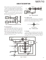
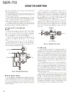
The TX VCO circuit consists of two VCOs (VCO A X58-
508: Q352, VCO B X58-508: Q353). Those VCOs generates
a transmit carrier. VCO A Q352 produces a transmitter fre-
quency from 136.000MHz to 154.995MHz. VCO B Q353
produces a transmitter frequency from 155.000MHz to
174.000MHz.
Those VCO oscillation frequencies are determined by
two systems of voltage control terminals: “CV” and “TXAS-
SIST”.
The voltage control terminals, “CV” and “TXASSIST”,
are controlled by the PLL IC (X58-508: IC300) and MCU
(X53-449: IC20) and the output frequency changes continu-
ously according to the applied voltage. For the modulation
input terminal, “MO”, the output frequency changes ac-
cording to the applied voltage.
D355
D352
D358
D359
SW Q350
TXVCOA
TX_CV
TXASSIST
TXVCOB
MO
80C
80C
VO
VCO_A
Q352
Buffer
Q354
SW Q351
D357
D353
D360
D361
VCO_B
Q353
Fig. 3 Transmitter VCO circuit
■
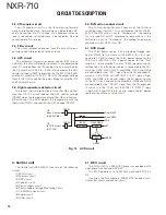
PLL IC (X58-508: IC300)
The PLL IC compares the differences in phases of the
VCO oscillation frequency and the transmitter PLL reference
signal (16.8MHz), returns the difference to the VCO CV ter-
minal and realizes the “Phase Locked Loop” for the return
control. This allows the VCO oscillation frequency to accu-
rately match (lock) the desired frequency.
When the frequency is controlled by the PLL, the fre-
quency convergence time increases as the frequency dif-
ference increases when the set frequency is changed. To
supplement this, the MCU is used before control by the
PLL IC to bring the VCO oscillation frequency close to the
desired frequency. As a result, the VCO CV voltage does not
change and is always stable at approx. 3.0V.
The desired frequency is set for the PLL IC by the MCU
(X53-449: IC20) through the 3-line “SPSD0”, “SPSCLK0”,
“/TXPCS” serial bus. Whether the PLL IC is locked or not is
monitored by the MCU through the “LDT” signal line. If the
VCO is not the desired frequency (unlock), the “LDT” logic
is low.
Ref 16.8MHz
LDT
SPSCLK0
SPSD0
/TXPCS
Buffer
Q300
TX VCO/PLL
IC300
LPF
TX_CV
BPF
FIN
Loop filter
Fig. 4 Transmitter Main PLL IC circuit
2-4. Modulation level adjustment circuit
The Modulation level adjustment circuit adjusts the mod-
ulation waveform balance. This circuit consists of IC804,
IC603, IC604, IC605 and IC606.
The modulating signal comes from the Control unit
(X53-449) through the interface connector (CN800 Pin 14).
The modulating signal is produced by the modulation low-
pitched tone to the transmitter modulation 16.8MHz PLL cir-
cuit and adds the high-pitched modulation to the transmitter
main PLL.
IC804 is an electronic volume control IC. It has 8 elec-
tronic volume control circuits. The modulation level adjust-
ment circuit uses 2 electronic volume control circuits in
IC804. The 1st electronic volume control circuit adjusts the
modulating signal and is fed to IC603 and the 2nd electronic
Fig. 2 Transmitter reference 16.8MHz PLL circuit
TX VCO
/PLL
MOD
PLL IC
X58-5080-10
Ref
10MHz
or 19.2MHz
LDT
IC602
SPSCLK0
SPSD0
/16_8PCS
AMP
Q602
Buffer
Q603
AMP
IC604
AMP
IC603
16.8MHz
LPF
Loop filter
X600
MB
OSC
16.8MHz
CIRCUIT DESCRIPTION


