NXR-710
15
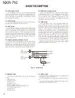
4-2. Memory circuit
The Memory circuit consists of the MCU (IC20), the
SRAM (IC9), and the fl ash memory (IC3).
The fl ash memory has a capacity of 32Mbit that contains
the transceiver control program for the MCU and stores the
data. It also stores the data for transceiver channels and
operating parameters that are written by the FPU. This pro-
gram can be easily written from external devices.
The SRAM has a capacity of 1Mbit that contains work
area and data area.
■
Flash memory
Note:
The fl ash memory stores the data that is written by
the FPU, tuning data (Deviation, Squelch, etc.), and firm-
ware program.
■
SRAM (static memory)
Note:
The SRAM has a temporary data area and work area.
When the power supply is off, it is backed up by an internal
secondary lithium battery. Therefore, the saved data is not
lost.
4-3. DSP circuit
The DSP circuit consists of a DSP (IC6) and processes
the base band signal. The DSP operates on an external clock
of 18.432MHz (the same as IC20). The I/O section operates
at 3.3V and the core section operates at 1.6V. The DSP car-
ries out the following processes:
■
Digital processing
• 4Level FSK and Baseband fi lter processing
• Vocoder processing between audio codec and modula-
tion/demodulation
• CAI processing, such as error correction encoding/decod-
ing and interleaving
• AFC loop control
• Frame synchronization and Time tracking
• Data scrambling
■
Analog FM processing
• Pre-emphasis/De-emphasis
• QT/DQT encoding/decoding
• DTMF encoding/decoding
• Compressor/Expander processing
• Voice scrambler processing
■
Audio or Modulation function
• Transmit/Receive audio fi ltering processing
• Microphone amplifi er AGC processing
• Audio soft mute processing
• Modulation level processing
• Squelch Filtering
■
Other function
• Voting tone
• CWID
• Courtesy tone
• Repeater operating
• Analog/Digital Mixed mode
4-4. Squelch circuit
The Squelch circuit amplifi es the demodulated noise sig-
nal from IC6 after fi ltering through the BPF circuit. The pro-
cessed digital noise signal is applied to CODEC IC14, and is
converted from digital to analog. The amplifi ed signal is then
converted to a DC signal by the detection circuit. The con-
verted signal is fed back to IC20.
Squelch
DAC
IC14
/PDN,
LRCLK,
SDTI,
BICLK
Buffer
IC16
VCTCXO
X1
(18.432MHz)
MAIN_CLK
XTAL_IN
ADC1
BSHIFT
/PCS_DSP
/SYMTIM, /DINT, /DWUP, FSDET, /HINT
MCSCKAF, /MCCSAF, MCDIAF, MCDOAF
/MCCSXCN, /MCCSRCN, MCDICN,
MCDOCN, MCSCKCN
A[0~17], D[0~7],
/RD, /WR, /CS2
A[0~21], D[0~15],
/RD, /WR, /CS0, /WP
A[0~20], D[0~15], /RD,
/WR, /HRDY, /CS3, /HDS2
VREF
AMP
IC13(A/2,B/2)
AMP
IC15(A/2)
AMP
Q4
LDR
/DRST
/FRST
/FRST
/DRST
33M 16M
33BU
33M
33M
33A
15M
FLASH
IC3
SRAM
IC9
DSP
IC6
MCU
IC20
Fig. 14 Control circuit
4-5. Power supply circuit
The X53-449 circuit consists of IC301, IC302, IC303,
IC304, IC305 and IC306.
IC301 is a DC/DC converter that converts 13.6V to 6.0V.
This 13.6V voltage is supplied from TX-RX unit (X57-794).
IC302 is connected to IC301 and regulates the voltage
to 5.0V. IC303, IC304, IC305 and IC306 are connected to
IC301. IC303 and IC306 are 3.3V voltage regulators. IC304
is a 1.5V regulator IC, and IC305 is a 1.6V regulator IC.
CN302 is the connector for the lithium battery. The
lithium battery is used to back up the SRAM and RTC data
when no external DC power source is available.
CIRCUIT DESCRIPTION


