NXR-901
12
CIRCUIT DESCRIPTION
3-1. Transmitter power amplifi er IC
The power amplifier MMIC is IC21. This device works
with linear operation mode and can operate from 700MHz to
2700MHz. The input and output matching circuit is adjusted
to the 935 to 941MHz band for the NXR-901. This device
does not have a gain control function, therefore the output
power is controlled by the drive power level.
The P1dB output power of the device is typically 28dBm
and its linear gain is typically 20dB.
The drive power from the TX unit is level controlled by
IC20, variable attenuator IC, to be fed into pin 1 and pin 2
of IC21 with matching circuit C302, C303 and the transmis-
sion line. The output terminals, pin 9 to 12 are matched to
50ohms with L30, C307, C310 and the transmission line.
To control the ramp-up and ramp-down waveform, the PA
VBIAS terminal voltage timing is managed by the PA_BIAS
signal and time constant circuit. IC6 (A/2) is the time con-
stant circuit.
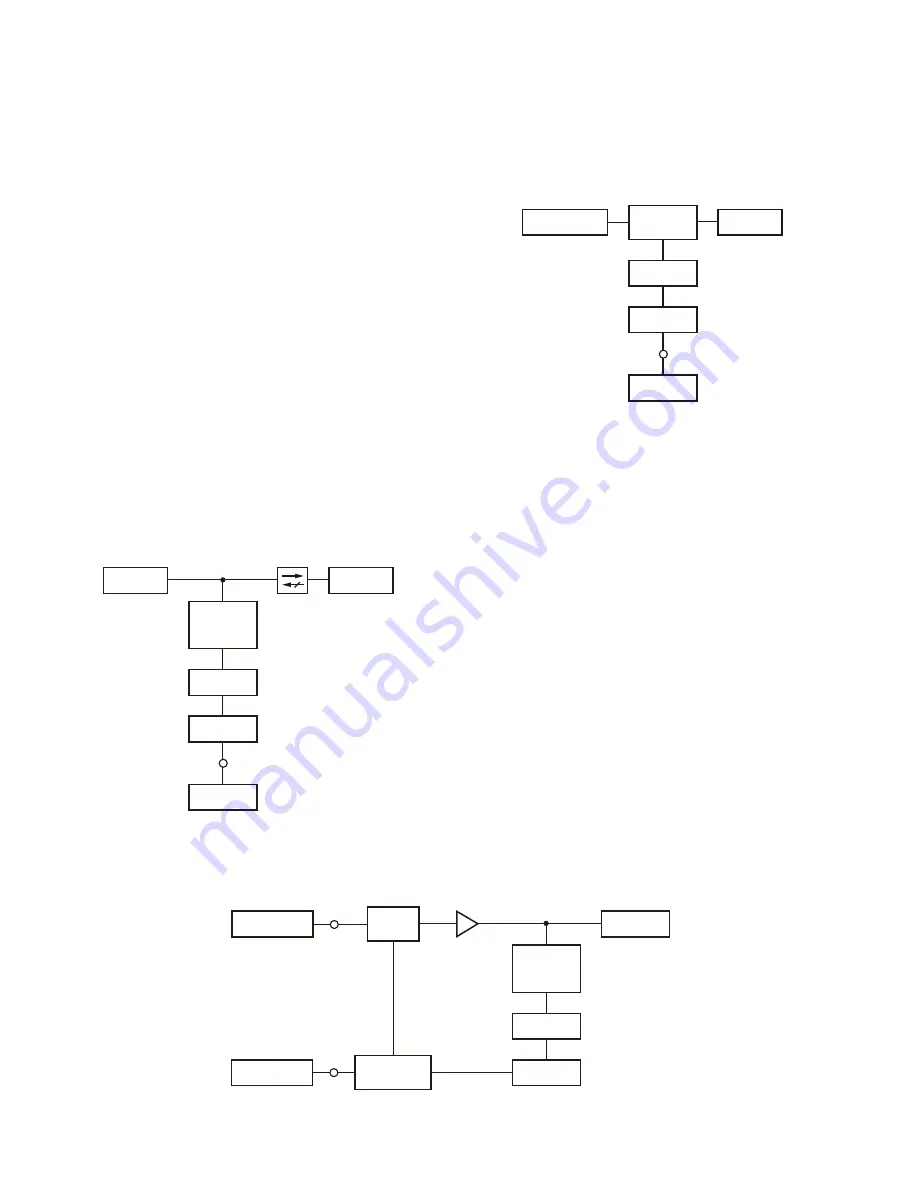
3-2. Forward power detector and isolator circuit
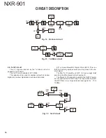
To stabilize the load impedance of IC21, an isolator de-
vice (L31) is used. Because there is very small reflection
power at the isolator input port, forward power coupling cir-
cuit is simplifi ed with C193 and R34, R38 and R42. Detected
DC voltage is amplifi ed by differential amplifi er IC4 (A/2).
RF signal
pick up
circuit
Detector
from PA
to Load
Amplifier
TX unit
CN20
#
9
IC4 A/2
D21
L31
Isolator
Fig. 7 Forward power detection circuit
3-3. Refl ected power detector circuit
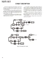
The reflected power detector circuit consists of a CM
coupling type detection circuit formed by a strip line and the
differential amplifi er IC4 (B/2).
Directional
coupler
Detector
from Isolator
to Load
Amplifier
TX unit
CN20
#11
IC4 B/2
D20
Fig. 8 Reverse power detection circuit
3-4. High pass fi lter and harmonic fi lter circuit
The T type single stage high pass fi lter prevents the PA
MMIC from being broken by static electricity. The harmonic
fi lter circuit uses a three-stage “pi” type Chebyshev LPF.
This circuit removes harmonics from the transmitter out-
put and sends the fi ltered signal to the antenna connector
(CN22).
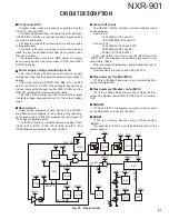
3-5. APC circuit
The APC circuit stabilizes the transmitter power so that
the output power specifi ed by the Control Voltage from the
MPU is obtained.
It consists of a Forward power detector circuit, Differential
amplifi ers (IC2) and a variable attenuator (IC20).
It compares the voltage detected by the Forward power
detector circuit (voltage detected by the Forward Power) and
the Control Voltage (PWR_CONT) from the MPU (IC802:
X56-315 A/3).
It stabilizes the output power by changing the drive power
of the PA MMIC (IC21). The attenuation value of IC20 is con-
trolled by the current value of pin 1 and pin 8.
The isolator consumes the refl ection power and the APC
controls the constant forward power under any TX antenna
terminal conditions. The antenna terminal load condition is
known by the refl ection detection circuit. Its detected voltage
relatively relates to the load VSWR value.
Differential
amplifier
Electric
ATT
to Isolator
from TX unit
from TX unit
RF signal
pick up
circuit
Detector
Amplifier
IC4 A/2
D21
IC2
IC20
IC21
CN1
CN20
#15
Fig. 9 APC circuit
Summary of Contents for NEXEDGE NXR-901
Page 154: ...1 E CN300 RX_IF_VN ...

