NXR-901
16
CIRCUIT DESCRIPTION
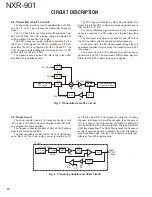
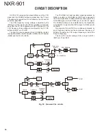
IC2 (PLL IC) compares the phase difference of the VCO
signal and the 20.0MHz reference signal from the TX unit.
The phase error signal from IC2 is fi ltered by the Q2 and Q3
active low pass fi lter.
The VCO frequency tuning voltage is adjusted by the
IC805 pin 3 DAC signal, the IC3 DC amplifi er and the low
pass fi lter. The LPF is confi gured with R32, C46 and D5. The
VCO frequency tuning voltage is monitored by the IC1 DC
buffer and IC811 pin 16 ADC.
The 2nd-PLL circuit consists of the VCO (Q604), the Buf-
fer amplifi er (Q609), the RF amplifi er (Q602), the RF doubler
(Q608) and the PLL-IC (IC603).
The 72.6MHz 2nd local oscillator signal generated by
Q604 is doubled to 145.20MHz by Q608 and is passed to
the LC band-pass fi lter to attenuate the spurious signals. The
145.2MHz signal is fed to IC603 (pin 5) as the Fin signal.
The 20.0MHz reference clock distributed by the Transmitter
unit (X56-315) is input as the REFin signal to IC603 (pin 8)
via Q602.
Two signals, Fin and REFin, are phase-compared by
each frequency divider as the comparison frequency of
200kHz. Therefore the VCO output frequency is half of the
PLL’s Fin frequency.
The 2nd VCO control voltage (CV2) is input to IC811
(ADC) pin 10 via IC601.
3dB
divider
PLL IC
Q5
Q
9
Active
LPF
Q2,Q3
IC805
DAC
IC3
IC811
ADC
IC1
IC2
823~82
9
MHz
823~82
9
MHz
20.0MHz
Q8
Q11
Q10
Q1
x2
x2
Frequency
doubler
Frequency
doubler
Ref signal
20MHz
1st mixer
411.5~414.5MHz
CV1
3dB
divider
3dB
divider
PLL IC
Q604
Q60
9
LPF
IC811
ADC
ATT
IC601
IC603
145.2MHz
20.0MHz
Q608
Q603
Q501
Q602
x2
Frequency
doubler
Ref signal
20MHz
CV2
72.6MHz
IC207
IC501
Fig. 18 Receiver PLL circuits
Summary of Contents for NEXEDGE NXR-901
Page 154: ...1 E CN300 RX_IF_VN ...


