NXR-901
19
CIRCUIT DESCRIPTION
The analog signal is output from pin 16 (AOUTR) of IC4.
The audio signal is then amplifi ed by IC12 (A/2), passed
through the low-pass filter at IC12 (B/2), selected by the
multiplexer IC14 (Y0=Y) and is then input into an electronic
volume IC8.
On the other hand, the transmitting audio signal output
from IC3 is amplifi ed by IC9 (A/4), applied to pin 3 (AINL) of
CODEC IC4, and is then converted from analog to digital at
a sampling frequency of 16.128kHz.
The digitized transmitting audio signal is AGC-processed,
pre-emphasized and filtered by DSP IC37, except for the
300Hz to 3kHz range, and is then fed back to CODEC IC4,
converted from digital to analog, and is then output from pin
15 (AOUTL).
The transmitting signal from the AOUTL is amplifi ed by
IC9 (B/4), passed through the IC9 (C/4) low-pass fi lter, and
is sent to the IC9 (D/4) summing amplifi er.
IC31 is a counter IC. The clock required for the CODEC
and DSP is generated by dividing the 16.515072MHz clock
signal supplied by the DSP IC37.
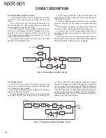
Fig. 21 An audio signal course and the frequency characteristic
■
Shift register circuit
The MPU (IC34) transmits serial data to shift registers
IC923 from IC923 to IC960 and from IC960 to IC963 in the
display circuit (X56-315 B/3, C/3).
Additionally, it transmits serial data to the Control unit
(X53-413) IC1 and IC22 and the Transmitter unit (X56-315)
IC703.
This serial data can control various functions of each unit.
■
Power supply circuit
This circuit consists of X53-413 IC6, IC10, IC11, IC15,
IC16 and IC18, and X53-414 IC305, IC306, IC307 and
IC329.
IC10 is a DC/DC converter that converts 13.8V to 5.0V.
IC11 is a DC/DC converter that converts 13.8V to 8.0V.
IC16 is connected to IC10 via the 5.0V AVR. IC6, IC15,
IC305 and IC329 are connected to IC329 via the 3.3V AVR.
IC18 is connected to IC329 via the 1.8V AVR. IC306 is con-
nected to IC329 via the 1.5V AVR. IC307 is connected to
IC15 via the 1.5V AVR.
■
Flash memory (RF control MPU)
IC17 is an 8M-bit Flash memory and contains MPU fi rm-
ware for controlling the RF.
■
EEPROMs circuit
The EEPROM is a built in Receiver unit (X55-312), Trans-
mitter unit (X56-315) and Final unit (X45-387).
The RF control MPU controls these EEPROMs via the
IIC bus.
6-2. X53-414
■
Main MPU
The Main MPU (IC703) is a 32-bit RISC microprocessor
incorporating a 16K bytes cache memory.
The main MPU controls the Flash memory, SDRAM,
SRAM, LAN IC, RS-232C driver, receiver and real-time clock
(RTC).
■
LAN interface
The NXR-901 is equipped with a 100Base-TX or 10Base-
T LAN interface. This circuit consists of IC719, IC720 and
J700. IC719 is a control IC. IC720 saves the MAC address in
the EEPROM. J700 is connected to the LAN cable.
■
Real time clock (RTC) circuit
This circuit consists of IC710 and X701. IC710 is a Real
Time Clock. X701 is a crystal oscillator.
IC710 is connected to IC703 (Main_MPU) via the IIC bus.
The oscillating frequency of X701 is 32.768kHz.
It is backed up by a secondary lithium battery (BA300).
The IC710 clock data is used after resetting the backup.
■
RS-232C circuit
The NXR-901 is equipped with a RS-232C interface.
It connects to a PC with a 9-pin female RS-232C cross
cable.
It uses the FPU and writes the fi rmware.
IC705 is a RS-232C driver receiver IC, and interfaces at
the RS-232C level.
CODEC IC
IC4: AK4550VTP
RX detected signal
(AINR)
(AOUTR)
(AOUTL)
(AINL)
RD
TA
TX modulation signal
Local Mic
2
3
REPEAT
RX
TX
16
15
TD
RA
RX audio amp.
TX VCO
(Modulation circuit)
300Hz
3kHz
[Frequency response]
RX
TX
REPEAT
(De-emphasis)
(Pre-emphasis)
(300Hz~3kHz Flat)
Summary of Contents for NEXEDGE NXR-901
Page 154: ...1 E CN300 RX_IF_VN ...

