1-102 (No.RA020<Rev.002>)
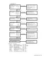
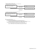
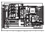
Verify the reference clock for the
BT/GPS.
(BT_CLK) Intersection of
C8 and C9: Sine waveform,
19.2MHz 0.2 to 1.2 Vp-p
[The reference clock circuit
for the BT/GPS is faulty]
When an abnormal
condition is confirmed.
When an abnormal
condition is confirmed.
When an abnormal
condition is confirmed.
When an abnormal
condition is confirmed.
When an abnormal
condition is confirmed.
When an abnormal
condition is confirmed.
When a normal
condition is confirmed.
When a normal
condition is confirmed.
When a normal
condition is confirmed.
When a normal
condition is confirmed.
When a normal
condition is confirmed.
When a normal
condition is confirmed.
X1, C4, C8, C9 (Whether not damaged)
Replace any abnormal parts.
Check the Module (BT/GPS) unit PCB side B.
Check the Module (BT/GPS) unit PCB side B.
Verify the ANT Matching Parts.
Visual check of R27, R29
(Whether not damaged)
Replace any abnormal parts.
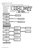
Verify the BT/GPS control signal
(BTFM_nSHUDoWN).
IC1 (5 pin): 1.8V
Check the Main unit PCB (a).
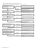
Verify the BT/GPS control
signal (TXD2).
CN1 (6 pin):
Square waveform UART data
of 3.3V logic.
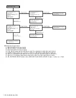
[The 18BT_HCI_RX(TXD2)
line circuit is faulty]
Visual check of the CP1, IC6, R22
(Whether not damaged)
Verify the BT/GPS control signal
(/BT_SHUTDOWN).
CN1 (14 pin): 3.3V
[/BT_SHUTDOWN Line circuit
is faulty]
Visual check of
the IC1, R7
(Whether not damaged)
Check the Main unit PCB (b).
Replace any abnormal parts.
Replace any abnormal parts.
Verify the BT/GPS control
signal (18BT_RX)
IC6 (7 pin):
Defeult: 115.2kbps
After: 3.967Mbps.
When a normal
condition is confirmed.
When a normal
condition is confirmed.
Visual check of the R9, Q1, R10, R26, R12, R13,
Square waveform UART data
of 1.8V logic.
Summary of Contents for NX-5700
Page 106: ...MEMO ...
Page 137: ...MEMO ...


