background image

PW-A

10

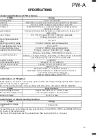
SPECIFICATIONS

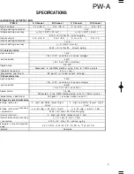
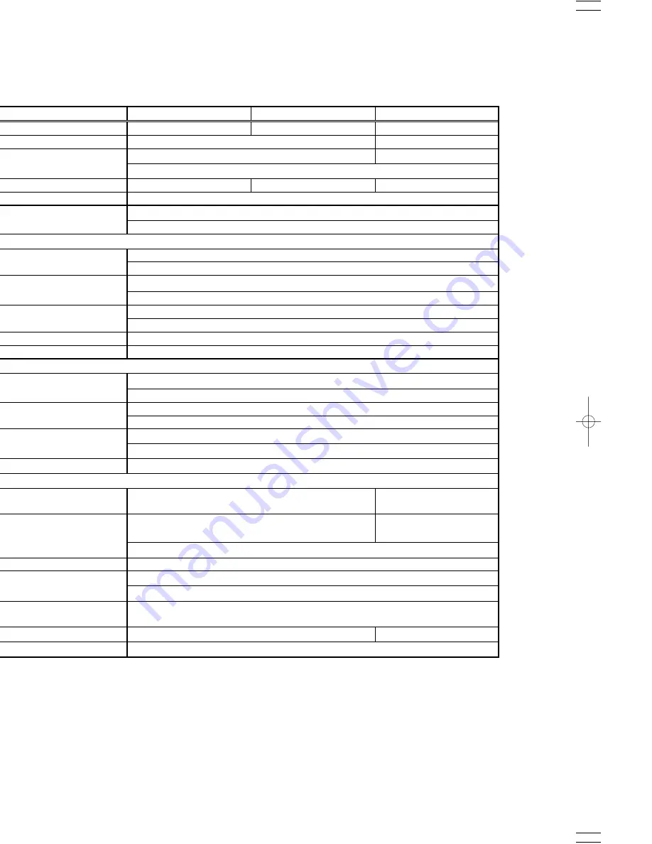
Specifications of PW8-3ATP 

ITEMS 

A Channel 

B Ch annel

C Ch annel 

Output voltage 

0 to +8 V 

0 to +8 V 

0 to +18 V 

Voltage setting  resolution 

1 mV 

10 mV 

±

( 0.5% SET +5 mV ) 

±

( 0.5% SET +20 mV ) 

Voltage setting  accuracy 


At 23 

±

5

°

C after 30-m

inute aging 

Output current 

0 to +3 A 

0 to +3 A 

0 to +1.5 A 

Current setting  resolution

1 mA 

±

( 1% SET +5 mA ) 

Current setting  accuracy 


At 23 

±

5

°

C  after 30-minute aging 

CV characteristics 

1 mV 

Input variation 

( For 

±

10% variation of source voltage) 

2 mV 

Load variation 

( For 0 to 100% variation ) 

0.5 mV   

Ripple noise 

Measured in the RMS method using 5 Hz to 1 MHz signals.   

Transient response 

50 

µ

s ( typ. ) 

Temperature coefficient 

60 ppm/

°

C ( at rated output voltage ) 

CC characteristics 

2 mA 

Input variation 

( For 

±

10% variation of source voltage) 

5 mA 

Load variation 

( For 0 to 100% variation ) 

1.5 mA   

Ripple noise 

Measured i n  the RMS


method  us ing  5 Hz t o  1 MH z  signals.

Temperature coefficient 

150 ppm/

°

C ( at rated output current ) 

Voltage & current   indication 

Voltage indicator 

4- digit red LEDs, lowest digit: 1 mV 


4- digit red LEDs, 

  lowest digit: 10 mV 

±

( 0.5% rdg + 5 mV )/ 1 mV 

±

( 0.5% rdg +20 mV ) 

/ 10 mV 

Voltage i ndication


accuracy & resolution 

At 23 

±

5

°

C  af ter 30-minute aging 

Current indicator 

4- digit red LEDs, lowest digit: 1 mA 

±

( 1% rdg + 5 mA )/ 1 mA 

Current i ndication


accuracy & resolution 

At 23 

±

5

°

C after 30-minute aging 

Voltage &  current 
indication range 

-2.5% FS to +102.5% FS /0% FS to +102.5% FS 

Common

 C ommon 

Independent 

Power consumption 

Approx. 215 W , 270 VA 

Summary of Contents for PW-A series

Page 1: ...161 00 K K PDF FILTER B11 0597 23 FRONT PANEL A63 0423 12 RUBBER FOOT J02 0363 04 KNOB ENCORDER K21 0907 14 KNOB BLUE K29 7260 02 KNOB RED K29 7257 02 KNOB BLACK K29 7258 02 KNOB WHITE K29 7259 02 KNOB RED K29 7257 02 SHORTING BAR E29 0506 04 COVER TOP F07 1538 03 REAR PANEL A83 0231 03 It changes by model ...

Page 2: ...perform any servicing other than contained in the operating instructions unless you are qualified to do so WARNING CONTENTS SPECIFICATIONS 3 CIRCUIT DESCRIPTION 15 BLOCK DIAGRAM 20 ADJUSTMENT 28 PRINTED CIRCUIT BOARD TABLE 34 PARTS LIST UNIT 35 PARTS LIST ELECTRICAL 38 SCHEMATIC DIAGRAM 57 P C BOARD 72 ...

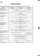
Page 3: ... Ripp le noise Measured in the RMS method using 5 Hz to 1 MHz signals Temperature coef ficient 150 ppm at rate d output current Voltage current indication Voltage indic ator 4 digit red LEDs lowest digit 10 mV 4 digit red LEDs lowest di git 1 mV 0 5 rdg 2 0 mV 10 mV 0 5 rdg 5 mV 1 mV Voltage indication accura cy accura cy resolution At 23 5 af ter 30 minute aging Curre nt indicator 4 digit red LED...

Page 4: ...riat ion 1 5 m A Measured in the RMS method using 5 Hz to 1 MHz sign als 150 ppm at rate d output current tage current indication age indicator 4 digit red LEDs lowest digit 10 mV 4 digit red LEDs lowest digit 1 mV 0 5 rdg 2 0 mV 10 mV 0 5 rdg 5mV 1 mV age indication indication accura cy accura cy esolution At 23 5 af ter 30 minute aging rent indicator 4 digit red LEDs low est di git 1 mA 1 rdg 5 ...

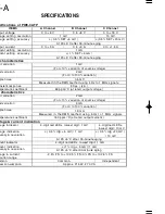
Page 5: ...rdg 2 0 mV 10 mV At 23 5 af ter 30 minute aging 4 digit red LEDs low est di git 1 mA 1 rdg 5 m A 1 mA At 23 5 after 30 minute aging 2 5 FS to 102 5 FS 0 FS to 102 5 Appr ox 2 15 W 274 VA ITEMS Channel A Channel B 10 Output voltage Output current Voltage setting resolution Current setting resolution Current setting accuracy Voltage setting accuracy CV characteristics Ripple noise nput variation Loa...

Page 6: ... ed LEDs lowest d igit 1 0 mV 0 5 rdg 2 0 mV 10 mV At 23 5 af ter 30 minute aging 4 digit red LEDs lowest di git 1 mA 1 rdg 5 m A 1 mA At 23 5 after 30 minute aging 2 5 FS to 102 5 FS 0 FS to 102 5 Appr ox 192 W 250 VA ITEMS Channel A Channel B 10 put voltage put current age setting resolution rent setting resolution rent setting accuracy age setting accuracy characteristics ple noise ut variation...

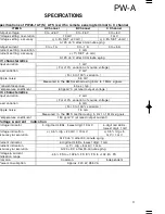
Page 7: ...z to 1 MHz signals Transient response 50 µs t yp Tem perature coefficient 60 ppm at rated output voltage at rated output current CC characteristics 2 mA 5 m A Load variation nput variation Load variation nput variation 1 5 mA Ripple noise Ripple noise Temperature coefficient 150 ppm 4 digit red LEDs lowest digit 10mV 4 digit red LEDs lowest digit 1mA 0 5 rdg 20 mV 10mV At 23 5 after 30 minute agin...

Page 8: ...on ent indication accuracy lution age ge current indication mmon Common wer consumption Approx 191W 242 VA 0 5 SET 5mV 0 5 SET 20mV At 23 5 after 30 minute aging At 23 5 after 30 minute aging 1 mA 1 SET 5mA 0 to 1A 0 to 2A 0 to 2A For 10 vari ation of source voltage For 10 variati on of source voltage For 0 to 100 variation Measured in the RMS method using 5 Hz to 1 MHz signals Measured in the RMS...

Page 9: ...ng resolution Current setting resolution Voltage setting accuracy Current setting accuracy CV characteristics Transient response Tem perature coefficient CC characteristics Load variation nput variation Load variation nput variation Ripple noise Ripple noise Temperature coefficient Current indicator Voltage indicator Voltage current indication Current indication accuracy esolution Voltage indicati...

Page 10: ...0 µs typ mperature coefficient 60 ppm C at rated output voltage characteristics 2 mA ut variation For 10 variation of source voltage 5 mA d variation For 0 to 100 variation 1 5 mA ple noise Measured i n the RMS method using 5 Hz t o 1 MHz signals mperature coefficient 150 ppm C at rated output current ltage current indication tage indicator 4 digit red LEDs lowest digit 1 mV 4 digit red LEDs lowes...

Page 11: ...s Transient response 50 µs typ Temperature coefficient 60 ppm C at rated output voltage CC characteristics 2 mA nput variation For 10 variation of source voltage 5 mA Load variation For 0 to 100 variation 1 5 mA Ripple noise Measured in the RM S method using 5 Hz t o 1 MHz signals Temperature coefficient 150 ppm C at rated output current Voltage current indication Voltage indicator 4 digit red LED...

Page 12: ...ponse 50 µs typ mperature coefficient 60 ppm C at rated output voltage characteristics 2 mA ut variation For 10 variation of source voltage 5 mA d variation For 0 to 100 variation 1 5 mA ple noise Measured in th e RMS method using 5 Hz to 1 MH z signals mperature coefficient 150 ppm C at rated output current ltage current indication tage indicator 4 digit red LEDs lowest digit 10 mV 0 5 rdg 20 mV ...

Page 13: ...ance Secondary casing 5 MΩ or more at 250 VDC o earth voltage 250 VDC reme dimentions mm 138 W x 124 H x 380 D Max dimentions mm 140 W x 147 9 H x 402 9 D Weight Approx 9 1 kg Accessories AC power cable 1 instruction manual 1 Lead wires with connectors for external contact control 1 Lead wires with sensing terminals PW18 1 3ATS PW26 1ATS only 2 pecifications of YB option he YB option is a vailable...

Page 14: ...ter IF 40RS r specifications are the same as those of the local bus PW bus munication Specifications of IF 40GU GP IB Block IB ctrical specifications Conforms to IEEE488 1978 hanical specifications Conforms to IEEE488 1978 rface functions SH1 AH1 T6 TE0 L3 LE0 SR1 RL1 PP0 DC0 DT0 C0 ress setting Possible to set address between 0 and 30 and listen only mode when turning on power d delimiters CR LF ...

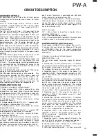
Page 15: ... setup LED is turned on by the driver a switch constitutes a matrix and scan is carried out from CPU Therefore the switch and LED are separated in circuit 8 Tact switch S13 14 19 20 23 Switch for an each setup The matrix is constituted with LED with switch and scan is carried out from CPU 9 Light Emitting Diode D3 11 LED for each display LED which displays the beam of output and setting change The...

Page 16: ... is shown in the following table X68 2210 2300 xx x E 6 23 The main power switch of a product is used It connects with a CPU unit X68 2210 2300 xx F 6 24 The switch 2 which switches the input AC of a product is used It is used in a CPU unit as A1 IFUNIT X72 154 The optional IF unit provides the PW A power supply unit with additional external control functions 0 00 is the IF 40GU 0 01 is the IF 40R...

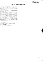
Page 17: ...is identical the description below explains channel 1 A number is a number of a block diagram 1 D A converter IC2 CH2 IC1 CH3 IC20 CH4 IC19 The D A converter receives digital signal indicating the set value from the CPU unit and converts it into an analog signal The PCM1700U a DAC unit used has two circuits which convert the CVREF voltage and CCREF voltage respectively The D A converter outputs ap...

Page 18: ... has a digital control circuit composed of a CPU ROM RAM and so forth AC inlet fuse input selector switch and AC power supply unit with capacitors The digital control circuit reads signals of the rotary encoder and switches from the display unit connected with a flat cable and sends control data to the amplifier unit The AC power supply unit feeds power input into the AC inlet to the transformer t...

Page 19: ...goes Low CN5 3 The voltage and current set values change into the PRESET3 values when this terminal goes Low CN5 4 The voltage and current set values change into the PRESET2 values when this terminal goes Low CN5 5 The voltage and current set values change into the PRESET1 values when this terminal goes Low CN5 7 The MAIN OUTPUT is turned off when this terminal goes Low It goes Low when the OHA co...

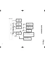
Page 20: ...T X73 2320 xx D A AD CONVERTING REF VO LTAGE AN ALOG CONTROL CIRCUIT POWER TRANSISTOR POWER TRANSFORMER POWER SUPPLY UNIT X68 2210 xx A 6 INTERNAL CIRCUIT POWER SUPPLY IF 40GU RS USB DC FAN OPTION FOR INTERFACE UNIT Y87 xxxx xx POWER SUPP LY UNIT X68 2210 xx D 6 RECTIFICATION CIRCUIT POWER SUPP LY UNIT X68 2210 xx C 6 SMOOTHING CIRCUIT 1 3 2 4 On output terminal a number changes model The power su...

Page 21: ...3 LED VOLTAGE DISPLAY ED1 4 D1 4 LED DRIVER IC2 5 LED CURRENT DISPLAY ED5 6 D2 6 LED DRIVER IC3 7 LED WITH SWITCH S1 12 S15 18 S21 S22 S24 8 TACT SWITCH S13 14 19 20 23 9 LED D3 11 R E A R E B CS0 CLK DATA CS2 CS1 ED1 ED2 LED KEY0 2 KEYD ATA0 7 CPU UNIT X77 2380 xx CN8 9 10 ...

Page 22: ...X68 2210 xx A 6 10 RECTIFIC ATION SMOOTING CIRCUIT D104 D105 C109 11 TRANSISTOR Q101 12 ERROR AMPLIFICATION CIRCUIT IC106 2 2 R107 108 109 110 DC FAN 7 REGUL ATOR CIRCUIT IC107 D108 8 HE AT DETECTION CIRCUIT TH101 9 OHA SIGNAL GENER ATING CIRCUIT IC106 X73 2320 xx AMP UNIT OUTPUT TERMINAL OUTPUT TERMINAL COM2 OUTPU T TERMINAL D OUTPUT TERMINAL TERMINAL X68 2210 xx B 6 S S OUTPUT TERMINAL OUTPUT TE...

Page 23: ...01 18 SMOOTHING CIRCUIT C302 16 RECTIFICATION CIRCUIT D402 X68 2210 xx D 6 20 SMOOTHING CIRCUIT C303 22 SMOOTHING CIRCUIT C304 19 POSITIVE NEGATIVE CHANGE W301 308 21 POSITIVE NEGATIVE CHANGE W309 316 X73 2320 xx AMP UNIT X68 2210 xx C 6 23 AC SWITCH S501 X77 2380 xx CPU UNIT X68 2210 xx E 6 X77 2380 xx CPU UNIT 24 SLIDE SWITCH S601 S602 X68 2210 xx F 6 ...

Page 24: ...NNEL 1 CONSTANT CURRENT CIRCUIT Q1 D1 3 19 R1 2 CHANNEL 2 CONSTANT CURRENT CIRCUIT Q2 D4 9 20 21 R3 4 CHANNEL 3 CONSTANT CURRENT CIRCUIT Q3 D10 15 22 23 R5 6 CHANNEL 4 CONSTANT CURRENT CIRCUIT Q4 D16 18 24 R7 8 AMP UNIT X73 2320 00 CN5 CN6 ...

Page 25: ...AMPLIFIER IC26 1 2 25 CV ERROR AMPLIFIER IC26 2 2 R166 R170 171 172 OR 26 POWER TRANSISTOR Q13 16 POWER SUPPLY UNIT X68 2210 D 6 27 CURRENT DETECTION CIRCUIT IC29 R189 R328 POWER SUPPLY UNIT X68 2210 B 6 C OUTPUT S COM 37 CC ERROR AMPLIFIER IC27 1 2 OR 39 POWER TRANSISTOR Q17 20 40 CURRENT DETECTION CIRCUIT IC30 R254 38 CV ERROR AMPLIFIER IC27 2 2 R231 R235 236 237 POWER SUPPLY UNIT X68 2210 B 6 2...

Page 26: ... DECODER IC6 X66 1820 00 PANEL UNIT 4 EEPROM IC4 5 2 RESET CIRCUIT IC11 ROM IC2 RAM IC3 6 ENCODER SIGNAL IC12 13 3 4 IC14 1 6 2 6 3 6 X72 1540 00 INTER FACE UNIT 7 OUTSIDE CONTROL CN5 Q1 Q2 POWER TRANSFORMER X68 2210 xx E 6 POWER SUPP LY UNIT 8 AC POWER J1 CN11 A1 C39 41 AMP UNIT X73 2320 xx ...

Page 27: ... PH1 IC14 GP IB CONTROL IC10 11 12 LOCAL BUS CONTROL IC13 S1 RS 232C LOCAL BUS CONTROL IC18 Q1 2 3 C17 21 USB TERMINAL J5 GP IB TERMINAL J1 LOCAL BUS TERMINAL J4 RS 232C TERMINAL J2 MODULAR TERMINAL J3 CPU UNIT X77 2380 xx CN8 9 10 IC5 6 7 8 4 5 6 7 8 ROM IC2 2 BUFFER BUS TRANSCEIVER ...

Page 28: ...1ATS Adjustment mode ID setting 1 Turn ON the power supply switch while pushing V key A key and MEMORY key Continue pushing Above key until the display called Idno X appears in a panel 2 Check the display Ajst Id X appears in a panel adjustment mode 3 Check whether the ID No display setting to adjust is correct refer to the following list MODEL NAME ID No MODEL NAME ID No PW18 1 8AQ ID No 1 PW16 5...

Page 29: ... that it becomes within the limits of the following list of the value of DMM 4 Press the MEMORY key MODEL NAME SETTING VOLTAGE ADJUSTMENT RANGE CH1 18 00 V CH2 18 00 V CH3 8 000 V PW18 1 8AQ CH4 6 000 V CH1 18 00 V CH2 18 00 V PW18 1 3AT CH3 6 000 V CH1 18 00 V PW18 3AD CH2 18 00 V CH1 36 00 V PW36 1 5AD CH2 36 00 V CH1 18 00 V PW18 3ADP CH2 18 00 V CH1 36 00 V CH2 18 00 V PW18 2ATP CH3 8 000 V CH...

Page 30: ...ss the MEMORY key MODEL NAME SETTING VOLTAGE ADJUSTMENT RANGE CH1 1 80 V 1 mV 1 mV 1 mV 1 mV 1 mV 1 mV 1 mV 1 mV 1 mV 1 mV 1 mV 1 mV 1 mV 1 mV 1 mV 1 mV 1 mV 1 mV 1 mV 1 mV 1 mV 1 mV 1 mV 1 mV 1 mV 1 mV 1 mV 1 mV 1 mV 1 mV 1 mV 1 mV CH2 1 80 V CH3 0 800 V PW18 1 8AQ CH4 0 600 V CH1 1 80 V CH2 1 80 V PW18 1 3AT CH3 0 600 V CH1 1 80 V PW18 3AD CH2 1 80 V CH1 3 60 V PW36 1 5AD CH2 3 60 V CH1 1 80 V P...

Page 31: ...3 Press the MEMORY key 4 Select the OUTPUT SELECT of the channel to adjust 1 Connect the output CH to adjust PWA and COM terminal to shunt register 2 Connect the sensing terminal of shunt register to DMM 1 Set up a current display in DIGIT key and a rotary encoder refer to the following list 2 Turn on MAIN OUTPUT 3 Adjust in DIGIT key and a rotary encoder so that it becomes within the limits of th...

Page 32: ... 0 500 V 1 Ω 1 Ω 1 Ω 1 Ω 1 Ω 1 Ω 1 Ω 1 Ω 1 Ω 1 Ω 1 Ω 1 Ω PW26 1ATS CH3 5 000 A 0 300 V 100 m Ω 100 m Ω 100 m Ω 100 m Ω 100 m Ω 100 m Ω 100 m Ω 100 m Ω 100 m Ω 5 Current rating 10 adjustment 1 Set up a current display in DIGIT key and a rotary encoder refer to the following list 2 Turn on MAIN OUTPUT 3 Adjust in DIGIT key and a rotary encoder so that it becomes within the limits of the following li...

Page 33: ... 1 000 V PW26 1ATS CH3 0 500 A 0 500 V current adjustment end when adjust other channels adjust in the same procedure from 5 4 2 ending current adjustment press the long pushing of KEYLOCK key more than 2 seconds cancel the current ment mode he end of adjustment complete all adjustments of the voltage current of each output turn OFF a power supply switch Or press the long pushing of KEYLOCK key 2 ...

Page 34: ... 02 OP 19B 01 01 PW36 1 5ADPYB Y87 4260 00 Y86 3460 00 OP 19H 07 07 MODEL NAME MODEL No INTERFACE UNIT X72 1540 xx IF 40GU Y87 4020 00 X72 1540 00 IF 40RS Y87 4030 00 X72 1540 01 IF 40USB Y87 4140 00 X72 1540 02 MODEL NAME MODEL No PANEL UNIT X66 1820 xx POWER SUPPLY UNIT X68 2210 xx POWER SUPPLY UNIT X68 2300 xx AMP UNIT X73 2320 xx CPU UNIT X77 2380 xx PW18 1 8AQ Y86 3090 00 02 00 00 00 PW18 1 3...

Page 35: ...nd E Europe G Germany Y AAFES Europe X Australia M Other Areas indicates safety critical components 02 Parts No Name Description A01 4125 01 1 1 CASE TOP A13 2280 11 1 1 FRAME A29 0526 04 1 1 PANEL A40 0733 01 1 1 CASE BOTTOM A63 0426 12 1 FRONT PANEL PW18 1 3AT A63 0469 02 1 FRONT PANEL PW18 1 3ATS A83 0231 03 1 1 REAR PANEL B09 0408 03 2 2 CAP B11 0600 23 1 1 FILTER B41 2083 04 1 1 CAUTION LABEL...

Page 36: ...01 1 1 PANEL UNIT X68 2210 07 1 POWER SUPPLY UNIT PW26 1AT X68 2210 11 1 POWER SUPPLY UNIT PW26 1ATS X73 2320 08 1 1 AMP UNIT X77 2380 01 1 1 CPU UNIT New Parts Parts without Parts No are not supplied Les articles non mentionnes dans le Parts No ne sont pas fournis Teile ohne Parts No werden nicht geliefert 3 00 L Scandinavia K USA P Canada R Mexico Y PX Far East Hawaii T England E Europe G German...

Page 37: ...rnis Teile ohne Parts No werden nicht geliefert 1 Name Description Parts No H 07 G 06 F 05 E 04 D 03 C 02 B 01 A 00 OP 19A H Y87 4150 XX L Scandinavia K USA P Canada R Mexico Y PX Far East Hawaii T England E Europe G Germany Y AAFES Europe X Australia M Other Areas indicates safety critical components Name Description B42 3820 05 LABEL Y87 4150 00 OP 19A PW18 1 8AQYB Y87 4150 01 OP 19B PW18 1 3ATY...

Page 38: ...INSULATOR SHEET AMP UNIT F20 3088 14 INSULATOR SHEET HEAT SINK H10 2906 15 FOAMED STYREN PAD FRONT H10 2907 15 FOAMED STYREN PAD REAR H13 1213 05 CARTON BOARD H20 1743 04 VINYL COVER H53 0368 03 CARTON BOX J02 0363 04 RUBBER FOOT J21 4843 04 BRACKET HANDLE Name Description J21 9047 04 BRACKET FET J21 9048 02 BRACKET POWER TRANSFORMER J59 0403 05 NYLON RIVET K01 0556 15 HANDLE K21 0907 14 KNOB ENCO...

Page 39: ...A101J RES CHIP 2 1 25 100 5 1 10W R5 1 1 1 RK73FB2A101J RES CHIP 2 1 25 100 5 1 10W R6 1 1 1 RK73FB2A101J RES CHIP 2 1 25 100 5 1 10W R7 1 1 1 RK73FB2A101J RES CHIP 2 1 25 100 5 1 10W R8 1 1 1 RK73FB2A101J RES CHIP 2 1 25 100 5 1 10W R9 1 1 1 RK73FB2A101J RES CHIP 2 1 25 100 5 1 10W R10 1 1 1 RK73FB2A101J RES CHIP 2 1 25 100 5 1 10W R11 1 1 1 RK73FB2A101J RES CHIP 2 1 25 100 5 1 10W R12 1 RK73FB2A...

Page 40: ...UNMOUNTED C101 1 1 1 1 1 1 1 1 1 1 1 CQ93FMG1H103J CAP PLASTIC FILM 0 01µ 5 50V C102 1 1 1 1 1 1 1 1 1 1 1 C90 4747 05 CAP ELECTRO 3300µ 20 25V C103 1 1 1 1 1 1 1 1 1 1 1 CQ93FMG1H103J CAP PLASTIC FILM 0 01µ 5 50V C104 1 1 1 1 1 1 1 1 1 1 C90 4749 05 CAP ELECTRO 2200µ 20 35V C104 1 C90 4750 05 CAP ELECTRO 3300µ 20 35V C105 1 1 1 1 1 1 1 1 1 1 C90 4749 05 CAP ELECTRO 2200µ 20 35V C105 1 C90 4750 05...

Page 41: ...k 1 1 6W R111 1 1 1 1 1 1 1 1 1 1 1 RN14BK2C6201F RES METAL FILM 6 2k 1 1 6W R112 1 1 1 1 1 1 1 1 1 1 1 RN14BK2C5601F RES METAL FILM 5 6k 1 1 6W R113 1 1 1 1 1 1 1 1 1 1 1 RD14BB2C471J RES CARBON 470 5 1 6W R115 1 1 1 1 1 1 1 1 1 1 1 RN14BK2C2201F RES METAL FILM 2 2k 1 1 6W R201 1 1 RD14DB3A182J RES CARBON 1 8k 5 1W R202 1 1 RD14DB3A182J RES CARBON 1 8k 5 1W R203 1 1 1 1 1 RD14BB2C100J RES CARBON ...

Page 42: ... 7292 05 PIN CONNECTOR 8P CN302 E40 7392 05 PIN CONNECTOR 6P CN303 E40 7292 05 PIN CONNECTOR 8P CN304 E40 7292 05 PIN CONNECTOR 8P CN401 E40 3367 05 PIN CONNECTOR 8P CN402 E40 3365 05 PIN CONNECTOR 6P CN403 E40 7669 05 PIN CONNECTOR 4P CN501 E40 7627 05 PIN CONNECTOR 5P CN502 E40 7627 05 PIN CONNECTOR 5P D101 S1VB20 DIODE D102 S1VB20 DIODE D104 DSM1D2 DIODE D105 DSM1D2 DIODE D106 MTZ16JB DIODE ZEN...

Page 43: ...D6413007F20 IC IC2 1 1 1 AT29C010A 12JI IC IC3 1 1 1 GM76C256CLLFW7 IC IC4 1 1 ML60851D IC New Parts Parts without Parts No are not supplied Les articles non mentionnes dans le Parts No ne sont pas fournis Teile ohne Parts No werden nicht geliefert 2 L Scandinavia K USA P Canada R Mexico Y PX Far East Hawaii T England E Europe G Germany Y AAFES Europe X Australia M Other Areas indicates safety cri...

Page 44: ... components Ref No Name Description 00 01 Parts No 02 R36 1 1 RS14DB2H151J RES METAL OXIDE FILM 150 5 1 2W R37 1 R92 0670 05 RES JUMPER 0 R38 1 1 RK73FB2A103J RES CHIP 2 1 25 10k 5 1 10W R39 1 1 RK73FB2A103J RES CHIP 2 1 25 10k 5 1 10W R40 1 1 1 RK73FB2A103J RES CHIP 2 1 25 10k 5 1 10W R41 1 1 RK73FB2A103J RES CHIP 2 1 25 10k 5 1 10W R42 1 1 RK73FB2A105J RES CHIP 2 1 25 1M 5 1 10W R51 1 R92 0670 0...

Page 45: ...D16 1SS133 1 DIODE D17 1SS133 1 DIODE D18 MTZ3 6JB 1 DIODE ZENER D19 1SS133 1 1 1 1 1 1 1 1 DIODE D20 1SS133 1 1 1 1 DIODE D21 1SS133 1 1 1 1 DIODE D22 1SS133 1 DIODE D23 1SS133 1 1 1 DIODE D24 1SS133 1 DIODE Q1 2SC5198 R 1 1 1 1 1 1 1 1 TR SI NPN Q2 2SA1941 R 1 1 1 1 TR SI PNP Q2 2SC5198 R 1 1 1 1 TR SI NPN Q3 2SA1941 R 1 1 1 TR SI PNP Q3 2SC5198 R 1 TR SI NPN Q4 2SA1941 R 1 1 1 1 TR SI PNP R1 RD...

Page 46: ...0 Ref No Parts No Name Description 1 1 1 1 1 1 1 1 1 1 J73 0752 12 PCB UNMOUNTED C1 1 1 1 1 1 1 1 1 1 1 CK73GF1E104Z CAP CERAMIC 0 1µ 20 80 25V C2 1 1 1 1 1 1 1 1 1 1 CK73GF1E104Z CAP CERAMIC 0 1µ 20 80 25V C3 1 1 1 1 1 1 1 1 1 1 CK73GF1E104Z CAP CERAMIC 0 1µ 20 80 25V C4 1 1 1 1 1 1 1 1 1 1 CK73GF1E104Z CAP CERAMIC 0 1µ 20 80 25V C5 1 1 1 1 1 1 1 1 1 1 CK73GF1E104Z CAP CERAMIC 0 1µ 20 80 25V C6 1...

Page 47: ...118 1 CK73GF1E104Z CAP CERAMIC 0 1µ 20 80 25V C119 1 CK73GF1E104Z CAP CERAMIC 0 1µ 20 80 25V C120 1 CK73GB1H103K CAP CERAMIC 0 01µ 10 50V C121 1 CK73GF1A105Z CAP CERAMIC 1µ 20 80 10V C122 1 1 1 1 1 CK73GF1E104Z CAP CERAMIC 0 1µ 20 80 25V C123 1 1 1 1 1 CK73GF1E104Z CAP CERAMIC 0 1µ 20 80 25V C124 1 1 1 1 1 CK73GF1E104Z CAP CERAMIC 0 1µ 20 80 25V C125 1 1 1 1 1 CK73GF1E104Z CAP CERAMIC 0 1µ 20 80 2...

Page 48: ...271J RES CHIP 2 1 25 270 5 1 10W New Parts Parts without Parts No are not supplied Les articles non mentionnes dans le Parts No ne sont pas fournis Teile ohne Parts No werden nicht geliefert 6 L Scandinavia K USA P Canada R Mexico Y PX Far East Hawaii T England E Europe G Germany Y AAFES Europe X Australia M Other Areas indicates safety critical components 09 08 07 06 05 04 03 02 01 00 Ref No Part...

Page 49: ...e Parts No werden nicht geliefert 8 L Scandinavia K USA P Canada R Mexico Y PX Far East Hawaii T England E Europe G Germany Y AAFES Europe X Australia M Other Areas indicates safety critical components 09 08 07 06 05 04 03 02 01 00 Ref No Parts No Name Description R17 1 1 1 1 1 1 RK73FB2A471J RES CHIP 2 1 25 470 5 1 10W R17 1 1 RK73FB2A751J RES CHIP 2 1 25 750 5 1 10W R18 1 1 1 1 1 1 1 1 1 1 RK73F...

Page 50: ...Y PX Far East Hawaii T England E Europe G Germany Y AAFES Europe X Australia M Other Areas indicates safety critical components 09 08 07 06 05 04 03 02 01 00 Ref No Parts No Name Description R81 1 1 1 1 1 1 1 1 1 1 RK73FB2A101J RES CHIP 2 1 25 100 5 1 10W R82 1 1 1 1 1 1 1 1 1 1 RK73FB2A103J RES CHIP 2 1 25 10k 5 1 10W R83 1 1 1 1 1 1 1 1 1 1 RN73FH2A153D RES METAL FILM 15k 0 5P 1 10W R84 1 1 RK73...

Page 51: ...on R140 1 1 1 1 1 1 1 1 1 1 RK73FB2A103J RES CHIP 2 1 25 10k 5 1 10W R141 1 1 1 1 1 1 1 1 1 1 RK73FB2A103J RES CHIP 2 1 25 10k 5 1 10W R142 1 1 1 1 1 1 1 1 1 1 RK73FB2A103J RES CHIP 2 1 25 10k 5 1 10W R143 1 1 1 1 1 1 1 1 1 1 RK73FB2A511J RES CHIP 2 1 25 510 5 1 10W R144 1 1 1 1 1 1 1 1 1 1 RK73FB2A102J RES CHIP 2 1 25 1k 5 1 10W R145 1 1 1 1 1 1 1 1 1 1 RK73FB2A152J RES CHIP 2 1 25 1 5k 5 1 10W R...

Page 52: ...ption R214 1 RK73FB2A242J RES CHIP 2 1 25 2 4k 5 1 10W R215 1 RN73FH2A103D RES METAL FILM 10k 0 5P 1 10W R216 1 RK73FB2A511J RES CHIP 2 1 25 510 5 1 10W R217 1 R92 0670 05 RES JUMPER 0 R219 1 R92 0670 05 RES JUMPER 0 R220 1 RK73FB2A242J RES CHIP 2 1 25 2 4k 5 1 10W R221 1 RN73FH2A302D RES METAL FILM 3k 0 5P 1 10W R222 1 RN73FH2A103D RES METAL FILM 10k 0 5P 1 10W R223 1 RK73FB2A511J RES CHIP 2 1 25...

Page 53: ... 5 1 10W R362 1 1 1 R92 0670 05 RES JUMPER 0 R363 1 1 1 R92 0670 05 RES JUMPER 0 R364 1 R92 0670 05 RES JUMPER 0 R365 1 1 1 1 1 R92 0670 05 RES JUMPER 0 R366 1 1 1 1 1 R92 0670 05 RES JUMPER 0 R367 1 R92 0670 05 RES JUMPER 0 R368 1 R92 0670 05 RES JUMPER 0 R369 1 RN73FH2A123D RES METAL FILM 12k 0 5P 1 10W R373 1 1 1 1 1 1 RK73FB2A473J RES CHIP 2 1 25 47k 5 1 10W R374 1 1 1 1 1 1 RK73FB2A473J RES C...

Page 54: ... sont pas fournis Teile ohne Parts No werden nicht geliefert 1 Ref No Name Description Parts No 05 04 03 02 01 00 1 1 1 1 1 1 E02 0217 05 SOCKET X X X X X X AT29C010A KW3 PROGRAMED ROM 1 1 1 1 1 1 J73 0753 12 PCB UNMOUNTED A1 1 1 1 1 1 1 W02 4057 04 SWITCH UNIT C1 1 1 1 1 1 1 C92 1547 05 CAP ELECTRO 100µ 20 10V C2 1 1 1 1 1 1 C92 1547 05 CAP ELECTRO 100µ 20 10V C3 1 1 1 1 1 1 CC73GCH1H100J CAP CER...

Page 55: ... Teile ohne Parts No werden nicht geliefert 4 Ref No Name Description Parts No 05 04 03 02 01 00 L Scandinavia K USA P Canada R Mexico Y PX Far East Hawaii T England E Europe G Germany Y AAFES Europe X Australia M Other Areas indicates safety critical components PH25 1 1 1 PC357NT IC PHOTO COUPLER PH26 1 PC357NT IC PHOTO COUPLER PH27 1 1 1 PC410 IC PHOTO COUPLER PH28 1 1 1 PC357NT IC PHOTO COUPLER...

Page 56: ...HIP 2 1 25 10k 5 1 10W R275 1 1 1 1 1 1 RK73FB2A103J RES CHIP 2 1 25 10k 5 1 10W R276 1 1 1 1 1 1 RK73FB2A103J RES CHIP 2 1 25 10k 5 1 10W R277 1 1 1 1 1 1 RK73FB2A103J RES CHIP 2 1 25 10k 5 1 10W R278 1 1 1 1 1 1 RK73FB2A103J RES CHIP 2 1 25 10k 5 1 10W R279 1 1 1 1 1 1 RK73FB2A103J RES CHIP 2 1 25 10k 5 1 10W R280 1 1 1 1 1 1 RK73FB2A103J RES CHIP 2 1 25 10k 5 1 10W R281 1 1 1 1 1 1 RK73FB2A103J...

Page 57: ...A C E G I B D F H J SCHEMATIC DIAGRAM PW A ...

Page 58: ...SCHEMATIC DIAGRAM L N P R T M O Q S PW A ...

Page 59: ...SCHEMATIC DIAGRAM U W Y AA AC V X Z AB AD PW A ...

Page 60: ...AF AH AJ AL AN AG AI AK AM SCHEMATIC DIAGRAM PW A ...

Page 61: ...AO AQ AS AU AW AP AR AT AV AX SCHEMATIC DIAGRAM PW A ...

Page 62: ...PW A Y39 4160 00 AY BA BC AZ BB ...

Page 63: ...BE BG BI BK BM BF BH BJ BL SCHEMATIC DIAGRAM PW A ...

Page 64: ...BN BP BR BT BV BO BQ BS BU BW SCHEMATIC DIAGRAM PW A ...

Page 65: ...schematic diagram for the value of resistors and capacitors OARD Component side view B D C E ER SUPPLY UNIT X68 2210 xx side view D 6 L UNIT X66 1820 xx side view rn side view INPUT UNIT X72 1620 xx Parts side view ...

Page 66: ...for the value of resistors and capacitors PC BOARD Component side view F H J G I POWER SUPPLY UNIT X68 2210 xx Parts side view B 6 Parts side Pattern side view F 6 Parts side Pattern side view A 6 Parts side view E 6 Parts side view C 6 ...

Page 67: ...or the value of resistors and capacitors OARD Component side view L N M O ER SUPPLY UNIT X68 2300 xx side view D 6 Parts side view C 6 side view E 6 Parts side view Pattern side view F 6 Parts side view B 6 side Pattern side view A 6 ...

Page 68: ...75 Refer to the schematic diagram for the value of resistors and capacitors PC BOARD Component side view P R T Q S INTERFACE UNIT X72 1540 xx Pattern side Parts side view Parts side Pattern side view ...

Page 69: ...Refer to the schematic diagram for the value of resistors and capacitors OARD Component side view V X W Y U UNIT X77 2380 xx ts side view ...

Page 70: ...77 Refer to the schematic diagram for the value of resistors and capacitors PC BOARD Component side view Z AB AD AA AC CPU UNIT X77 2380 xx Pattern side Parts side view ...

Page 71: ...AE AG AI AK AM AF AH AJ AL AN Refer to the schematic diagram for the value of resistors and capacitors PC BOARD Component side view 78 79 AMP UNIT X73 2320 xx Parts side Parts side view Pattern side ...

Page 72: ...PW A A product of KENWOOD TMI CORPORATION 1 16 2 HAKUSAN MIDORI KU YOKOHAMA CITY 226 8525 JAPAN ...

Reviews: