TK-3102G
9
CIRCUIT DESCRIPTION
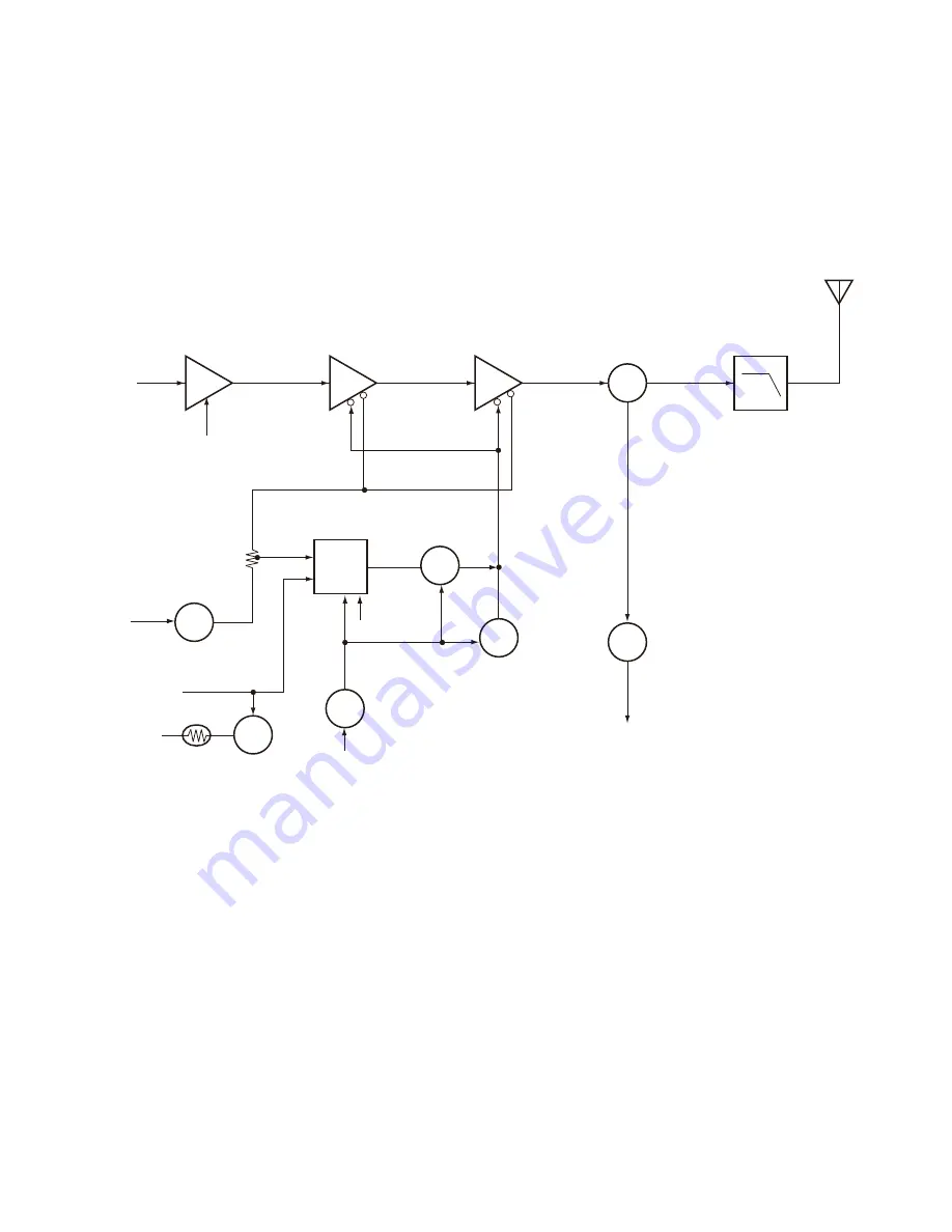
3) VCO and RF Amplifi er
The transmit signal obtained from the VCO buffer ampli-
fier Q100, is amplified by Q101 and Q102. This amplified
signal is passed to the power amplifier, Q105 and Q107,
which consists of a 2-stage FET amplifi er and is capable of
producing up to 4W of RF power. (See Fig. 7)
4) ANT Switch and LPF
The RF amplifi er output signal is passed through a low-
pass fi lter network and a transmit/receive switching circuit
before it is passed to the antenna terminal. The transmit/
receive switching circuit is comprised of D101, D102 and
D103. D102 and D103 are turned on (conductive) in transmit
mode and off (isolated) in receive mode.
5) APC
The automatic power control (APC) circuit stabilizes the
transmitter output power at a predetermined level by sens-
ing the drain current of the fi nal amplifi er Field Effect Tran-
sistor (FET) . The voltage comparator, IC100 (2/2), compares
the voltage obtained from the above drain current with a
reference voltage which is set using the microprocessor.
An APC voltage proportional to the difference between the
sensed voltage and the reference voltage appears at the
output of IC100 (1/2). This output voltage controls the gate
of the FET power amplifier, which keeps the transmitter
output power constant. The transmitter output power can
be varied by the microprocessor which in turn changes the
reference voltage and hence, the output power.
6) Thermal Protection Circuit
When the thermistor (TH102) reaches about 80°C, the
protection circuit turns on Q110 to protect transmitting fi nal
amplifi er (Q107) from the over heating.
5. Power Supply
A 5V reference power supply [5M] for the control circuit
is derived from an internal battery. This reference is used
to provide a 5V supply in transmit mode [5T], a 5V supply in
receive mode [5R], and a 5V supply common in both modes
[5C] based on the control signal sent from the microproces-
sor.
6. Control System
The IC403 MPU operates at 7.37MHz . This oscillator has
a circuit that shifts the frequency according to the EEPROM
data.
Fig. 7 APC system
AMP
Q101, Q102
DRIVE AMP
Q105
5T
B
Q103,104
B SW
DET
IC100
APC
5T
Q109
SW
Q106
SW
APC
5T
Q108
SW
RX
D102,103
ANT SW
FINAL AMP
Q107
ANT SW
D101
LPF
ANT
5T
SW
Q110
TH102


