background image

17

TK-782

"

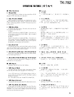
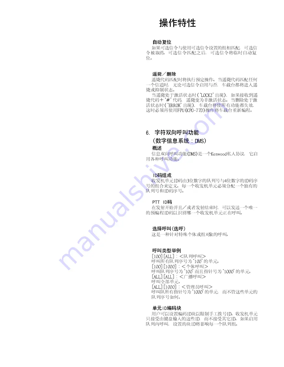
Auto Reset

If option signalling matches a group set up with option

signalling, option signalling is released.  After matching op-
tion signalling, option signalling will temporarily reset auto-
matically.

"

Stun/Kill

If the stun code matches, a predetermined action will oc-

cur.  Whether option signalling is activated or not, when stun
code matches on any channel, the transceiver will become
stun or kill.

While stun is active (“LOCK2” appears), if the stun code +

“#” code is received, stun will disactive.  While kill is active
(“ERROR” appears), the transceiver will be disable all func-
tions.  The transceiver must be reprogrammed by the FPU
(KPG-77D) to operation again.

6. Alphanumeric Two-way Paging Function

(Digital Message System : DMS)

"

General

The Alphanumeric Two-way Paging Function (DMS) is a

Kenwood proprietary protocol.  It enables a variety of paging
functions.

"

ID Construction

A radio unit ID is defined by a combination of 3-digit Fleet

and 4-digit ID numbers.  Each radio unit must be assigned its
own Fleet and ID numbers.

"

PTT ID

A pre-programmed unique ID can be sent at the begin-

ning of transmission and/or the end of transmission to iden-
tify which radio unit is on air.

"

Selective Call (SELCALL)

This is a voice call to a particular individual or group of

stations.

!

Example of call types;

[100][ALL ] : <Fleet Call>
All the units whose fleet number is “100” are called.
[100][1000] : <Individual Call>
The unit, whose the fleet number is “100” and ID number
is “1000”, is called.
[ALL][ALL ] : <Broadcast Call>
All the units are called.
[ALL][1000] : <Supervisor Call>
All ID “1000” are called regardless of their fleet number.

!

Unit ID Encode Block

Encode ID Block can be set to limit manual dial ID.  The

radio unit will not accept an ID other than these IDs which
are entered from the keypad.  If Inter-fleet Call is enabled,
block ID setting affects  each fleet group.

OPERATING FEATURES / 

"

"

"

"

"

"

!

!

Summary of Contents for TK-782

Page 1: ...been taken in the preparation of this manual Kenwood assumes no responsibility for errors or omissions Neither is any liability assumed for damages resulting from the use of the information contained herein Kenwood reserves the right to make changes to any products herein at any time for improvement purposes 文档版权信息 Kenwood Corporation 拥有版权 2006 保留所有权利 未经 Kenwood 公司预先书面同意 无论出于何种目的 均不得以任何形式或任何方式包 括电...

Page 2: ...MENT 59 TERMINAL FUNCTION 76 PC BOARD VIEWS PLL VCO X58 4712 71 78 TX RX UNIT X57 6143 01 A 2 79 TX RX UNIT X57 6143 01 B 2 85 SCHEMATIC DIAGRAM 89 BLOCK DIAGRAM 97 LEVEL DIAGRAM 100 SPECIFICATIONS 102 CONTENTS VHF FM TRANSCEIVER VHF Cabinet Upper A01 2165 23 Panel assy A62 0642 03 Key top K29 9105 22 2 5 23 28 35 42 45 49 57 58 59 77 PLL VCO X58 4712 71 78 TX RX UNIT X57 6143 01 A 2 79 TX RX UNIT...

Page 3: ...within two feet 0 6 meter of the antenna DO NOT transmit until all RF connectors are verified se cure and any open connectors are properly terminated SHUT OFF and DO NOT operate this equipment near elec trical blasting caps or in an explosive atmosphere All equipment should be properly grounded before power up for safe operation This equipment should be serviced by a qualified techni cian only PRE...

Page 4: ...Check the vehicle ground polarity before installa tion to prevent wasted time and effort 2 Connect the positive power lead directly to the vehicle battery positive terminal Connecting the Positive lead to any other positive voltage source in the vehicle is not rec ommended 3 Connect the ground lead directly to the battery negative terminal 4 The cable provided with the radio is sufficient to handl...

Page 5: ... the following precaution The rating of pin 7 SB of the accessory connector cable KCT 19 on the rear of the radio is 13 6V 0 75A Insert a 1A fuse if you use the SB pin for external equipment Accessory connector cable KCT 19 If you do not intend to use the 3 5 mm jack for the exter nal speaker fit the supplied speaker jack cap B09 0235 05 to stop dust and sand getting in 1 3 7 6 13 15 Speaker jack ...

Page 6: ...ower is switched on again the transceiver returns to the previous conditions CHANNEL UP DOWN key CALL key Programmable key Programmable A B C and D key Programmable VOLUME UP DOWN key Programmable BUSY TX LED The BUSY indicator Green LED shows that the channel is in use The TX indicator Red LED shows that you are transmitting 2 2 Programmable Keys The FPU KPG 77D enables programmable keys to selec...

Page 7: ...e lower level AUX B This function can be programmed when the voice scram bler board is not installed If this key is pressed an underscore _ appears at the extreme right of the LCD and OPT port which is inside of the transceiver turns to the active level low If pressed again the underscore disappears and the OPT ports turns to the deactive level high Channel Name Press this key to switch between th...

Page 8: ... when Fixed volume key is pressed When Fixed volume key is pressed tone level changes in turn to low tone volume low high tone volume high and off Group Up Down When this key is pressed each time the group number to be selected is increased decreased and repeats if held for one second or longer Home Channel Press this key once the channel switches to the preprogrammed home channel Key Lock Key loc...

Page 9: ... the microphone When you are in Queue mode D or 6 key to toggle the Selcall and Status displays When you are in Queue mode press the C or 4 key to toggle the Code and Selcall Status displays Hold down the D or 6 key to delete the top stack of the Queue buffer Hold down the C or 4 key to cancel Queue mode and return to normal operation Radio Password Backup is done even if the power supply is cut o...

Page 10: ...lcall Status List Select the selcall number you wish to call Press Selcall Status list key to enter Selcall list select mode It works as Status list mode If you press Selcall Status list key again it works as Status list select mode Send GPS You can send the GPS location data manually To perform the operation you have to install a GPS receiver with NMEA 0183 output GPS receiver must be installed S...

Page 11: ... ON or OFF keys Press these keys to activate their programmable auxiliary functions page 11 Display See page 10 for more information keys Press these keys to activate their programmable auxiliary functions page 11 Microphone jack Insert the microphone plug into this connector A B C D and CALL keys Press these keys to activate their programmable auxiliary functions page 11 Display Indicator Descrip...

Page 12: ...s the channels that are not locked out of the scanning sequence Selective Call is a dealer programmable optional function Rear Panel Programmable Auxiliary Functions Keys and page 10 can be programmed with the auxiliary functions listed below Please contact you dealer for further details on these functions Auto Dial None Autodial Programming Operator Sel Tone AUX A Queue AUX B Scan Channel Down Sc...

Page 13: ...tware or when the monitor signalling cancel function is activated Scan channel types 1 Priority channel is the most important channel for the scan and always detects a signal during scan and when the scan stops temporarily 2 Non priority channels detects a signal during scan For the channels that can be selected with the group or chan nel up down key when the scan does not occur adds an indicator ...

Page 14: ...scan icon SCN and SCAN or revert channel programmable display goes off Temporarily delete add It is possible to delete or add channel temporarily during scan When scan stops on unnecessary channel for example by interference of the other party activate the delete add func tion for example press the key then that channel is deleted temporarily and scan re start immediately When you would like to ad...

Page 15: ...ignal type is the type of active low or high for the PLL unlock logic signal Com port Com 0 This function selects the external serila port function at the microphone jack TXD RXD PC programming is ac cepted regardless of this setting Com 1 This function selects the external COM1 pin serial port function on the KCT 19 accessory jack If the transceiver is installed GPS unit this function must be set...

Page 16: ...ransceiver unless enter the correct password This code can be up to 6 digits from 0 to 9 and input with the key and CALL key Off hook decode If the Off hook decode function has been enabled remov ing and replacing the microphone on the hook has no effect for decoding QT DQT and option signalling Timed power off This function works as Automatic Power Switch Off Timed power off timer starts from the...

Page 17: ...use individual call group call stun kill Stun and kill are used with DTMF If the option signalling matches a predetermined action will occur If option signalling matches on a group channel which is set up with option signalling the option signalling indicator will flash and option signalling will be released The transpond or alert tone will sound If the selective call alert LED is set up the orang...

Page 18: ...les a variety of paging functions ID Construction A radio unit ID is defined by a combination of 3 digit Fleet and 4 digit ID numbers Each radio unit must be assigned its own Fleet and ID numbers PTT ID A pre programmed unique ID can be sent at the begin ning of transmission and or the end of transmission to iden tify which radio unit is on air Selective Call SELCALL This is a voice call to a part...

Page 19: ...cy Status Note Remote stun works with DTMF stun function also Automatic Status Response If you pre select a status number and leave the radio in the Status Mode it can automatically respond with the se lected status number upon request from the base station The request function is initiated by serial control on the base station Optional Short Messase Optional A maximum of 48 characters can be sent...

Page 20: ...o call a radio with a different fleet number radio users can manually dial a unit ID with a different fleet number Status Short Long Message on Data Group Channel Status Short Long Message transmission is made whether on the Data Group Channel Status Short Unit ID Message Serial Output Whether a received Status Short message or PTT ID is outputed or not to serial port GPS Report A NMEA 0183 GPS un...

Page 21: ...essages to be sent before transmitting a data message if it is being made on Data Group Channel If a radio unit receives a GTC mes sage it will move to the Data Group Channel of the current group Increase this item to make sure the called radio unit moves to the Data Group Channel Random Access Contention When a channel is busy radio unit will not transmit de pending on its Busy Channel Lockout se...

Page 22: ...ime is the amount of time from the beginning of transmission to the beginning of a data modulation It is used every time data is transmitted 7 Audible User Feedback Tones The transceiver outputs various combinations of tones to notify the user of the transceiver operating state The main tones are listed below Power on tone This tone is output when the transceiver is turned on The high tone is outp...

Page 23: ...rror tone Sounds when a key is pressed but that key cannot be used Roll over tone Sounds at the smallest group channel Transpond tone Sounds when an individual call with the correct DTMF option signalling is received For group calls only the group tone will sound not the transpond tone Pre alert tone Sounds prior to the TOT TX inhibit activation If TOT pre alert is set the tone sounds at the amoun...

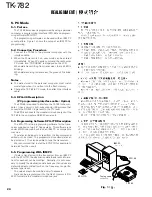
Page 24: ...ram ming mode of the flash memory Clone mode Used to transfer programming data from one radio to another Self programming Frequency signalling and features write mode to the radio 2 How to Enter Each Mode Mode Operation User mode Power ON Panel test mode B Power ON PC mode Received commands from PC Panel tuning mode Panel test mode A Firmware programming mode A Power ON Clone mode D Power ON Self ...

Page 25: ...ector 25 pin case that converts the RS 232C logic level to the TTL level The KPG 46 connects the modular microphone jack of the TK 782 to the computers RS 232C serial port 5 4 Programming Software KPG 77D Description The KPG 77D is the programming software for the trans ceiver supplied on two 3 5 floppy disks This software runs under MS Windows 95 or 98 on an IBM PC or compatible machine The data ...

Page 26: ...y the LED on the TK 782 lights and the checksum is displayed 8 If you want to continue programming other TK 782 re peat steps 4 to 7 Notes This mode cannot be entered if the Firmware program ming mode is set to Disable in the Programming software KPG 77D When programming the firmware it is recommend to copy the data from the floppy disk to your hard disk before up date the radio firmware Directly ...

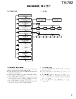
Page 27: ...isplayed information is not stored in memory and the next item appears Press to return to the original display SELF PROG The setup items for channel setting mode are listed be low Setup function Display Remarks 3 character Channel selection CH or GRP RX frequency RXF CALL Switches frequency on off B Changes the step value between 5kHz 6 25kHz and 1MHz RX signalling RXS CALL Switches between off QT...

Page 28: ...X signalling REALIGNMENT 7 2 Flow Chart 7 3 Memory Reset Mode You can clear all settings you made in self programming mode or you can return to the original display Press A while SELF PROG is displayed will change the display to CLEAR NO Press Channel up down to change the display between CLEAR NO and CLEAR YES When CLEAR YES is displayed pressing A will set all data to default and ALL CLEAR will ...

Page 29: ...ssis 2 Remove the pad as shown in Figure 1 2 3 Insert the KCT 19 cable 3 into the chassis 4 The wire harness band 5 must be inside the chassis 4 Replace the DC cord bushing 6 5 Connect the KCT 19 to the TX RX unit A 2 as shown in Figure 2 7 6 Connect the KCT 19 to the external accessory by inserting the crimp terminal 8 into the square plug 9 both of which are supplied with the KCT 19 1 2 1 3 13 1...

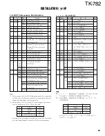
Page 30: ...put 1 and active low 2 CN4 CN2 AM Speaker mute input 14 E 2 CN4 RXD Serial control data input 2 CN2 MM MIC mute input active high 15 E 3 CN4 TXD Serial control data output 2 CN2 DTC Data control channel signal input 1 Data channel Low LOK TX logic signal output active low TXS Transmitter sense output Active high FSW Foot switch input active low Note 1 The functions of A 2 A 5 A 13 when connector E...

Page 31: ...s No TXS No Yes MI Default LOK AM R5 0Ω R6 0Ω Function Default Yes No AM Default No Yes LOK DTC LOK TXS FSW R168 R84 R51 R13 Function Default 0Ω 0Ω 0Ω 0Ω No No No Yes LOK Yes No No No DTC Default No No Yes No TXS No Yes No No FSW Note The following parts are not installed at the time of shipping R6 R12 R13 R51 R84 and R94 Fig 3 INSTALLATION R51 R13 R12 R167 R24 R94 R168 R6 R5 R84 TX RX unit A 2 Fo...

Page 32: ...can select Carrier operate relay or Tone operate relay Active logic level or type can select in the KPG 77D CN2 1 AM I Audio mute signal input LOK O TX logic signal output Active logic level is low Active type can be selectable in the KPG 77D 2 MM I MIC mute input 3 DTC I Data control channel signal input Data channel L Normal channel H TXS O Signal indicating whether the trans ceiver is transmitt...

Page 33: ...n control unit when the scrambler board is attached The table below shown the differences between the sche matic terminals and the PC board terminals Schematic diagram PC board view Name I O Function Name Unit SB O Switched B 13 6V 0 75A SB TX RX A 2 5C O 5C 5C TX RX A 2 GND Earth E TX RX A 2 DEO O Detect signal output Output DEO TX RX A 2 level 250mVrms standard modulation RXAI I RX audio input R...

Page 34: ...t used C4 TX RX A 2 SQ O Squelch signal output Signal SQ TX RX A 2 logic type can select Carrier operate relay or Tone operate relay Active logic level or type can select in the KPG 77D TXD1 O Serial data output 1 TD1 TX RX A 2 RXD1 I Serial data input 1 RD1 TX RX A 2 TXD2 O Serial data output 2 TD2 TX RX A 2 RXD2 I Serial data input 2 RD2 TX RX A 2 RSSI O Receive signal strength indication RSSI T...

Page 35: ...he TX RX unit B 2 control section Fig 5 2 Fold the flat cable 1 in the opposite direction 2 3 Rotate the control section 3 180 degrees 4 4 Insert the flat cable into the control section connector CN502 5 5 Mount the control section on the transceiver 6 CN502 1 2 3 4 5 6 Fig 6 Fig 5 INSTALLATION 1 2 3 4 5 6 6 Rotate the control panel 180 degrees and mount it on the transceiver Refit the two halves ...

Page 36: ...passes through a low pass filter and a transmission reception selection diode switch D211 D212 and goes to the front end of the receiver The front end filter is a variable BPF consisting of three coils and three varicap diodes D206 D207 D208 to eliminate unwanted out of band signal components The low noise amplifier LNA Q202 uses a bipolar transistor to achieve wide band and low distortion amplifi...

Page 37: ...gnal output from the D A converter is added with the BEEP signal BPO and the resulting signal is input to the audio power amplifier IC10 The AF signal from IC10 switches between the internal speaker and speaker jack J1 output CF1 Wide CF2 Narrow IFI MXO IC11 IF system AFO DET OUT C107 C100 C108 R114 R123 R133 R126 R125 R130 R131 Q16 DM Q32 R121 W N IC7 11pin Wide H Narrow L C118 D22 D23 Q23 5C Q24...

Page 38: ... Q300 and goes to the PLL IC IC300 The modulation signal from CN101 is applied to D109 and passes through C125 and C126 to modulate the carrier The PLL IC uses a fractional N type synthesizer to improve the C N ratio and lock up speed The VCO output signal in put to the pin 5 of the PLL IC is divided to produce a compari son frequency according to a channel step This signal is compared with the re...

Page 39: ...l is goes the antenna terminal APC Circuit The automatic transmission power control APC circuit detects part of a power module output with a diode D27 D30 and applies a voltage to Q21 Q21 compares the APC control voltage PC generated by the D A converter IC5 and DC amplifier IC6 with the detection output voltage to con trol Q19 and Q20 generates DB voltage from B voltage and stabilizes transmissio...

Page 40: ... bit EEPROM IC512 The flash ROM contains firmware programs data and user data which is programmed with the FPU The EEPROM contains adjustment data The CPU IC511 controls the flash ROM through an external ad dress bus and an external data bus The CPU controls the EEPROM through two serial data lines Fig 10 Momory circuit SCL SDA IC511 CPU ADDRESS BUS DATA BUS IC510 FLASH ROM IC512 EEPROM Fig 11 Dis...

Page 41: ...ssor according to the data AFDAT from the CPU The signal is summed with a MIC MSK signal by the audio processor IC504 and the re sulting signal passes through an analog switch IC506 and goes to the TX RX unit A 2 MO MO is summed with the external pin DI line by the sum ming amplifier IC3 and the resulting signal goes to the D A converter IC5 The D A converter IC5 adjusts the MO level and the balan...

Page 42: ...4 on Q4 can sink a maximum of 100mA Fig 15 Horn control 8C HOR D7 Q4 Q6 R58 Q5 R2 R50 R152 B IC7 Shift register HNC IGN Power Supply Circuit When the POWER switch on the control unit is pressed the PSW signal goes low This signal is inverted by Q26 and sent to a flip flop IC IC15 This IC outputs a control signal when the PSW goes low When the power turns on pin 1 of IC15 outputs a low signal and Q...

Page 43: ...utput timing pulse input 17 AFRTM I FFSK demodulation data input tim ing pulse input 18 MICDAT O MIC key data output 19 CP O PLL IC clock output 20 BEEP O Beep data output 21 AFRDT I FFSK demodulation data input 22 AFREG1 O AF IC register switching data output 1 23 AFREG2 O AF IC register switching data output 2 24 EEPDAT O EEPROM data output 25 EN O D A converter IC data strobe output 26 AFCLR O ...

Page 44: ...ss bus 62 VSS GND 63 70 A7 A0 Flash memory address bus 71 74 KEY1 KEY4 I O Key matrix data input output 1 4 75 MINDAT O Common data output 76 78 KEY5 KEY7 I Key matrix data input 5 7 79 86 D7 D0 Flash memory data bus 87 DTMDAT I DTMF decode IC data input 88 AUXDTC I External DTC input 89 MICBLC O MIC back light control output 90 POWSW I Power switch input 91 ANLSQL I Squelch level input 92 PTT I P...

Page 45: ...eat shift H ON L OFF 13 Q6 KEY TX power switching H TX L RX 14 Q5 T R TX RX switching H RX L TX 15 OE Output enable 16 VDC 5V Terminal function TX RX unit A 2 IC7 Pin No Port Name Function 1 STB ES Strobe 2 SI DT Data 3 CLK CK Clock 4 Q1 HORN Horn alert H ON L OFF Auxiliary A H ON L OFF 5 Q2 HL RF power switching H High L Low 6 Q3 TIMOFF Timed power off H Power off 7 Q4 NC 8 VSS GND 9 NC 10 NC 11 ...

Page 46: ...ontrol IC9 5V AVR External 5C IC10 AF power amp IC11 FM IF DET Quadrature detector 2nd mixer OSC IF amplifier RSSI IC12 5V AVR 5C IC13 9V AVR 9C Terminal function TX RX unit A 2 IC8 Pin No Port Name Function 1 STB ES Strobe 2 SI DT DATA 3 CLK CK Clock 4 Q1 AM1 Audio mute 1 H Mute L Unmute 5 Q2 LOK Link complete Programmable active H L 6 Q3 STR VCO shift switching H TX L RX 7 Q4 DM DET mute H RX L ...

Page 47: ...me on Q13 8T SW control KEY H time on Q15 IF amp 44 85MHz Q16 DET output level Wide time on switch Q17 PC switch TX 8T time on Q18 DET mute KEY H time on Q19 APC APC driver Q20 APC APC pre driver Q21 APC control Q22 TOF switch TOF H time on Q23 W N switch Wide time off Q24 W N switch Wide time on Q25 TOF switch Q22 on time on Q26 Inverter Power switch L time on Q27 SB switch Q28 on time on Q28 SB ...

Page 48: ...orption B D34 Protection DC 20V and over time on D35 Charge DEO D37 Reverse protection D40 41 Charge Ripple filter D206 208 BPF tune D209 210 Usable temperature range D211 ANT swtich TX time on D212 ANT switch TX RX Unit X57 6143 01 B 2 Control Section Ref No Use Function Operation Condition IC501 LPF amplification LSD IC502 Amplification AF HSD IC503 Base voltage ASQ Buffer amp IC504 Audio proces...

Page 49: ...15 Key backlight switch D501 Surge absorption BLC D502 Over current PSB protection D503 Surge absorption CM D504 Surge absorption PTT TXD D505 Surge absorption HOOK RXD D507 OR gate MIC mute MM MM1 D508 Limiter MIC D509 Limiter ASQ D510 Reverse current C575 charge protection D511 BUSY TX LED Busy time green on TX time red on Green Red D512 517 Key backlight KBLC H time on D518 Current regulation K...

Page 50: ...C 10PF D C20 CK73GB1E103K CHIP C 0 010UF K C21 22 CK73GB1H102K CHIP C 1000PF K C23 C92 0507 05 CHIP TAN 4 7UF 6 3WV C24 CK73GB1H102K CHIP C 1000PF K C25 C92 0507 05 CHIP TAN 4 7UF 6 3WV C27 CK73GB1H102K CHIP C 1000PF K C28 CC73GCH1H470J CHIP C 47PF J TK 782 C29 C92 0628 05 CHIP TAN 10UF 10WV C30 CK73GB1H102K CHIP C 1000PF K C31 C92 0628 05 CHIP TAN 10UF 10WV C32 CC73GCH1H220J CHIP C 22PF J C33 CK7...

Page 51: ... C176 177 CC73GCH1H470J CHIP C 47PF J C181 CK73GB1H102K CHIP C 1000PF K C182 C92 0565 05 CHIP TAN 6 8UF 10WV C188 CK73GB1H102K CHIP C 1000PF K C196 198 CK73GB1H102K CHIP C 1000PF K C199 CC73GCH1H080D CHIP C 8 0PF D C201 CK73GB1H102K CHIP C 1000PF K C202 C93 0550 05 CHIP C 1 0PF C C204 CK73GB1E103K CHIP C 0 010UF K C207 208 CK73GB1H102K CHIP C 1000PF K C209 CK73GB1C104K CHIP C 0 10UF K C210 CK73GB1...

Page 52: ... CHIP C 390PF J C541 CC73GCH1H100D CHIP C 10PF D C542 CC73GCH1H391J CHIP C 390PF J C543 CK73GB1H272K CHIP C 2700PF K C544 CC73GCH1H030C CHIP C 3 0PF C C545 CK73GB1H102K CHIP C 1000PF K C546 CK73GB1H122K CHIP C 1200PF K C547 CK73GB1H102K CHIP C 1000PF K C548 C92 0560 05 CHIP TAN 10UF 6 3WV C549 CK73GB1C104K CHIP C 0 10UF K C550 CC73GCH1H101J CHIP C 100PF J C552 CK73GB1C333K CHIP C 0 033UF K C553 CK...

Page 53: ...SMALL FIXED INDUCTOR 47NH L501 508 L92 0138 05 FERRITE CHIP X1 L77 1766 15 VCXO 16 8MHZ X2 L77 1762 05 CRYSTAL RESONATOR 44 395MHZ X501 L77 1708 05 CRYSTAL RESONATOR 3 579545MHZ X502 L78 0462 05 RESONATOR 9 8304M XF1 L71 0572 05 MCF 44 85MHZ CP501 R90 0724 05 MULTI COMP 1K X4 R1 RK73GB1J102J CHIP R 1 0K J 1 16W R2 R92 1252 05 CHIP R 0 OHM J 1 16W R3 4 RK73GB1J102J CHIP R 1 0K J 1 16W R5 R92 1252 0...

Page 54: ...155 RK73GB1J333J CHIP R 33K J 1 16W R156 RK73GB1J471J CHIP R 470 J 1 16W R157 RK73GB1J101J CHIP R 100 J 1 16W R158 RK73GB1J473J CHIP R 47K J 1 16W R161 RK73GB1J474J CHIP R 470K J 1 16W R162 163 RK73FB2A103J CHIP R 10K J 1 10W R164 RK73GB1J122J CHIP R 1 2K J 1 16W R165 R92 1252 05 CHIP R 0 OHM J 1 16W R167 168 R92 1252 05 CHIP R 0 OHM J 1 16W R169 RK73GB1J154J CHIP R 150K J 1 16W R170 R92 0670 05 C...

Page 55: ...73GB1J182J CHIP R 1 8K J 1 16W R546 RK73GB1J224J CHIP R 220K J 1 16W R547 RK73GB1J103J CHIP R 10K J 1 16W R548 RK73GB1J183J CHIP R 18K J 1 16W R550 RN73GH1J682D CHIP R 6 8K D 1 16W R551 RK73GB1J223J CHIP R 22K J 1 16W R552 RK73GB1J334J CHIP R 330K J 1 16W R553 RK73GB1J102J CHIP R 1 0K J 1 16W R554 RK73GB1J332J CHIP R 3 3K J 1 16W R555 RK73GB1J474J CHIP R 470K J 1 16W R556 RK73GB1J223J CHIP R 22K J...

Page 56: ...9 DA204U DIODE D8 9 HSB123 DIODE D11 DAN202U DIODE D12 14 DA204U DIODE D12 14 HSB123 DIODE D15 DAN235E DIODE D16 1SS355 DIODE D17 DA204U DIODE D17 HSB123 DIODE D20 1SS355 DIODE D21 02DZ5 6 X Y ZENER DIODE D22 23 DAN235E DIODE D24 MINISMDC075 02 VARISTOR D26 1SS355 DIODE D27 HSM88AS DIODE D28 02DZ15 X Y ZENER DIODE D30 HSM88AS DIODE D31 1SS355 DIODE D32 22ZR 10D SURGE ABSORBER D34 02DZ18 X Y ZENER ...

Page 57: ...106 2SC4215 Y TRANSISTOR Q13 DTC114EE DIGITAL TRANSISTOR Q15 2SC2059K P TRANSISTOR Q16 DTC144EE DIGITAL TRANSISTOR Q17 2SC2412K S TRANSISTOR Q18 2SK1824 FET Q19 2SD2394 TRANSISTOR Q20 2SB1188 Q TRANSISTOR Q21 FMW1 TRANSISTOR Q22 DTC114EE DIGITAL TRANSISTOR Q23 DTA114EE DIGITAL TRANSISTOR Q24 DTC144EE DIGITAL TRANSISTOR Q25 26 DTA114EE DIGITAL TRANSISTOR Q27 2SA1641 S T TRANSISTOR Q28 29 DTC114EE D...

Page 58: ...1 20 6 42 13 28 15 2 28 3 16x2 31 J1 TX RX unit A 2 TX RX unit B 2 Cx2 704 701 702 B B Cx2 Dx11 Ax2 C C 703 703 A A 32 A M2 6 x 6 OC BLK N32 2606 45 B M3 x 8 N67 3008 46 C M2 6 X 6 Br Tap N87 2606 46 D M2 6 x 12 Br Tap N87 2612 46 Parts with the exploded numbers larger than 700 are not supplied ...

Page 59: ...tion manual B62 1659 00 33 Polystyrene foamed fixture F H10 6618 12 34 Polystyrene foamed fixture R H10 6619 12 37 Protection bag H25 0720 04 38 Item carton case H52 1930 02 Parts with the exploded numbers larger than 700 are not supplied ...

Page 60: ...Shift off Channel Up Down Shift off Volume Up Down Shift off Controls SFT not appears PTT Used when making a transmission Monitor on and off A Sets to the tuning mode B Shift on C RF power high and low D Changes signalling CALL Changes wide and narrow Channel Up Down Changes channel Volume Up Down Volume up down Note If a A B C D key is pressed during trans mission the DTMF corresponding to the ke...

Page 61: ...023N DQT 023N 8 DQT 754I DQT 754I 9 DTMF DEC 159D DTMF ENC 159D 10 None DTMF tone 9 11 None Single tone 1200Hz 12 None FFSK 13 FFSK code FFSK code Preparations for tuning the transceiver Before attempting to tune the transceiver connect the unit to a suitable power supply Whenever the transmitter is turned the unit must be con nected to a suitable dummy load i e power meter The speaker output conn...

Page 62: ...RF power high 3 point tuning ex Maximum deviation Narrow F R E Q 1 Adjustment item Adjustment 1 256 F R E Q 1 FREQ xxx D HPOW xxx B LPOW xxx n BAL xxx w BAL xxx CALL 5 point tuning 5 point tuning 3 point tuning n MAX xxx w MAX xxx CALL 3 point tuning n QT xxx w QT xxx w DQT xxx CALL 3 point tuning n DQT xxx CALL w DTMF xxx n DTMF xxx CALL w FFSK xxx n FFSK xxx CALL w TONE xxx n TONE xxx CALL B 3 p...

Page 63: ...ity Frequency Range 10Hz to 1000MHz Frequency Counter Frequency Stability 0 2ppm or less 7 Ammeter 20A 8 AF Volt Meter Frequency Range 50Hz to 10kHz AF VTVM Voltage Range 1mV to 10V 9 Audio Generator AG Frequency Range 20Hz to 20kHz or more Output 0 to 1V 10 Distortion Meter Capability 3 or less at 1kHz Input Level 50mV to 10Vrms 11 4Ω Dummy Load Approx 4Ω 10W or more 12 Regulated Power Supply 13 ...

Page 64: ...TK 782 1 8 1 BLC 2 PSB 3 E 4 PTT 5 ME 6 MIC 7 HOOK 8 CM 63 ...

Page 65: ...viation Squelch etc for the EEPROM is stored in memory When parts are changed readjust the transceiver Measurement Test equipment Unit Terminal Adjustment Unit Parts Method Specifications Remarks Condition Item 1 PLL lock 1 Set test mode DVM TX RX TP1 PLL TC101 1 5V Receive 0 1V voltage CH CH3 Sig1 Power meter A 2 PTT OFF Receive TC102 1 5V Transmit PTT ON Transmit 2 CH CH2 Sig1 Check 8 0V or less...

Page 66: ...C SOURCE BUSY TX LED VOLUME UP VOLUME DOWN CHANNEL UP CHANNWL DOWN SUB DISPLAY MONITOR PRIORITY SERVICE AUXILIAY HANDSET SCAN MAIL PROGRAMMABLE FUNCTION KEYS ALPHANUMERIC DISPLAY L203 L204 L202 L6 VR1 TX RX UNIT A 2 PLL VCO TC101 TP1 TC102 ...

Page 67: ...r SSG MOD 1 5kHz Oscilloscope AF output 1V 4Ω AG 2 C SENS SSG freq 226 050MHz 3 H SENS SSG freq 234 950MHz 3 Squelch 1 Set test mode Squelch must be Select nL SQL in tuning mode closed once SSG freq 217 050MHz Then adjust for SSG output Sensitivity squelch open point value of 12dB SINAD SSG MOD 1 5kHz Narrow 2 nC SQL SSG freq 226 050MHz 3 nH SQL SSG freq 234 950MHz 4 wL SQL wC SQL wH SQL SSG freq ...

Page 68: ...TK 782 67 ...

Page 69: ...0MHz SSG output 70dBm SSG MOD 1 5kHz Narrow 2 nC HRSI SSG freq 226 050MHz 3 nH HRSI SSG freq 234 950MHz 4 wL HRSI wC HRSI wH HRSI SSG freq 70dBm SSG output Sensitivity value of 12dB SINAD SSG MOD 3 0kHz Wide 6 Squelch 1 Set test mode Check Squelch must be opened check CH CH1 Sig1 Wide Narrow SSG freq 226 050MHz SSG output 15dB SINAD level 2 SSG output OFF Squelch must be closed Wide Narrow 7 QT ch...

Page 70: ...TK 782 69 ...

Page 71: ...2 L2 HPOW PTT ON 3 C HPOW PTT ON 4 H2 HPOW PTT ON 5 H HPOW PTT ON 4 Low power 1 Set test mode Power meter 5 0W 0 5W Select LPOW in tuning mode L LPOW PTT ON 2 L2 LPOW PTT ON 3 C LPOW PTT ON 4 H2 LPOW PTT ON 5 H LPOW PTT ON 5 Power check 1 Set test mode Power meter ANT Check 25W 1W 8A or less CH CH1 Sig1 CH2 Sig1 Ammeter DC IN CH3 Sig1 PTT ON 6 Modulation 1 Set test mode Power meter Rear ANT Make t...

Page 72: ...TK 782 71 ...

Page 73: ...anel LPF 15kHz HPF OFF De emphasis OFF PTT ON 2 nC MAX PTT ON 3 nH MAX PTT ON 4 w MAX PTT ON 8 MIC 1 Set test mode Check 3kHz 0 2kHz Wide seisitivity CH CH1 Sig1 1 5kHz 0 05kHz Narrow check AG 1kHz 4mV PTT ON 9 QT deviation 1 Set test mode 0 75kHz Wide 50Hz Wide Narrow Select QT in tuning mode 0 35kHz Narrow nL QT Deviation meter filter LPF 3kHz HPF OFF PTT ON 2 nC QT PTT ON 3 nH QT PTT ON 4 w QT ...

Page 74: ...TK 782 73 ...

Page 75: ...1kHz Narrow Deviation meter filter meter LPF 15kHz Oscilloscope HPF OFF PTT ON AF VTVM Front MIC AG panel 2 w DTMF PTT ON 12 FFSK 1 Set test mode 3 0kHz Wide 0 1kHz Wide Narrow deviation Select n FFSK in tuning mode 1 5kHz Narrow Deviation meter filter LPF 15kHz HPF OFF PTT ON 2 w FFSK PTT ON 13 TONE 1 Set test mode 3 0kHz Wide 0 1kHz Wide Narrow deviation Select n TONE in tuning mode 1 5kHz Narro...

Page 76: ...TK 782 75 ...

Page 77: ...N DA converter enable 26 APTT External PTT 27 CP PLL clock 28 DTC Data control 29 TXD Serial data 30 RXD Serial data 31 OE Serial data 32 FSW Foot switch 33 E Ground CN101 PLL VCO TX RX Unit A 2 Pin No Name Function 1 ST Switched transmit input H Transmit 2 HT RF output 3 E Ground 4 9CL 9V input 5 8CL 8V input 6 MD Modulation input 7 CV Control voltage input CN501 TX RX Unit B 2 Pin No Name Functi...

Page 78: ...TK 782 77 ...

Page 79: ...7 Q102 G S D G S D Q103 L103 C114 L104 R116 C110 R101 R107 C104 R108 R105 L110 L109 C122 R109 C127 C129 C134 C135 C136 C138 L106 Q104 Q105 Q106 Q101 C111 L105 C120 C125 C133 R103 D109 C143 CN101 CV MD 8CL 9CL E HT ST J72 0732 02 C107 C106 C121 C103 C102 C117 C119 R110 C108 R102 C126 C115 L101 C105 R117 R106 R104 C113 R115 R113 L102 R114 R111 C130 D101 D102 R118 D104 C131 C132 C139 C142 D107 R119 R...

Page 80: ...R77 C75 D9 VR1 R127 R122 R179 C140 C401 R403 R402 R401 C402 C131 CN4 D12 D13 D8 C70 C319 R314 R313 C318 C314 C309 C307 C311 R310 C37 C306 C4 C8 C13 C5 C2 C3 C6 C9 C7 C90 C38 C41 C97 Q401 C125 C296 C312 R309 R121 C100 R129 R98 R58 Q302 Q301 R300 C36 R190 R302 R305 R303 R301 R2 R50 R68 L5 C316 R312 R323 R311 C48 C28 R30 R44 R414 R111 Q21 1 3 4 5 R55 C321 Q17 R80 C68 R76 G IC14 I O R85 10 C109 C112 R...

Page 81: ...IC1 4 1 5 8 IC9 I G O S D G C65 C120 C42 C80 IC6 1 4 8 5 C121 C78 C144 R69 L230 D20 D26 R39 Q12 R62 R106 PA R90 R130 R36 R408 R52 R28 R29 R131 R104 L3 C55 D23 R107 R31 R22 R140 R153 R26 R27 D15 C30 R34 Q22 Q25 Q29 Q9 C146 C148 C181 Q204 Q203 E C B E C B R147 D212 C237 D211 C255 C231 C235 C240 C241 C282 C243 C261 C274 C273 C251 IC400 1 2 3 4 D210 R223 C290 C289 C272 C271 R224 R230 R238 C242 R250 R2...

Page 82: ...108 D22 R45 R42 C73 C76 D16 R144 R406 R9 R151 R138 R146 L4 C69 L1 Q23 Q24 Q26 Q28 Q30 Q31 R157 C135 C138 C145 C141 C147 C139 C149 C209 C238 IC201 1 3 4 5 R229 C207 C208 C229 C230 C232 C279 C233 C277 C234 C278 C280 C281 C176 C236 C239 C288 C407 C406 C202 D209 L211 L212 Q202 B C E R211 R212 R213 R214 R217 R220 R221 R228 R231 R232 R233 R234 R236 R237 R240 L225 C124 C128 C134 C136 C29 C157 R154 C155 R...

Page 83: ...R721 R724 R725 CN501 1 10 Q501 CN502 33 1 L501 L502 L504 L505 L508 Q515 E 5C CS CK SID NC NC LEDA LEDK NC E FSW OE RXD TXD DTC CP APTT EN EP ES LD RSSI DT CK KEY 8C SB SB IGN AHK MI ME AFO MM DEO PSW 8R BEEP TO MO T R W N IC508 CM MIC PTT TXD PSB BLC D513 E ME HOOK RXD R682 C592 C583 IC501 1 1 4 4 5 5 8 8 C513 C535 IC503 R507 C518 IC502 D517 R517 C593 C511 R508 C527 C575 R545 R551 D512 D515 D516 R...

Page 84: ...BEEP TO MO T R W N E 5C CS CK SID NC NC LEDA LEDK NC Q515 IC508 CM MIC PTT TXD PSB BLC D513 E ME HOOK RXD R682 C592 C583 IC501 1 1 4 4 5 5 8 8 C513 C535 IC503 R507 C518 IC502 D517 R517 C593 C511 R508 C527 C575 R545 R551 D512 D515 D516 R514 R510 R612 R572 1 8 9 16 C524 R525 R526 C506 R502 C574 D510 D520 R548 C540 C547 R552 R523 R531 Q511 C510 C710 C712 1 1 8 4 5 3 4 5 C714 IC710 R710 R713 R714 R726...

Page 85: ...T R P N L J H F D B S Q O M K I G E C A 1 3 5 7 2 4 6 SCHEMATIC DIAGRAM TK 782 Note Components marked with a dot are parts of layer 1 92 ...

Page 86: ...A C E G I K M O Q S B D F H J L N P R T 1 3 5 7 2 4 6 TK 782 SCHEMATIC DIAGRAM Note Components marked with a dot are parts of layer 1 93 ...

Page 87: ...TK 782 TK 782 TK 782 99 BLOCK DIAGRAM ...

Page 88: ...m 25W SG input level for 12dB SINAD are obtained measured by connecting SG to each point via a 0 01µF capacitor AF VTVM AF level obtained when the AF output level is adjusted for 0 45V 4Ω with the front panel AF VOL control Measured with AF voltmeter connected to the external speaker jack receiving a 53dBm SSG signal modulated at 1kHz DEV 3kHz Wide 1 5kHz Narrow X58 4712 71 Wattmeter by 50Ω 1 AG i...

Page 89: ... x 145 D mm 0 94kg RECEIVER Measured by TIA EIA 603 Antenna Impedance 50Ω Sensitivity EIA 12dB SINAD 0 25µV Selectivity Wide 80dB Narrow 70dB Intermodulation Wide 75dB Narrow 65dB Spurious and Image Rejection 80dB Audio Output 4W at 4Ω less than 10 distortion Channel Frequency Spread 15MHz RX Switching Time 25ms TRANSMITTER Measured by TIA EIA 603 RF Power Output 5W 25W Spurious Emission 36dBm 1GH...

Page 90: ...103 TK 782 1 DEO 2 AHK 3 NC 4 DI 5 ME 6 MI 7 PTT 8 SQ E37 0854 15 CN1 1 AM 2 MM 3 DTC 1 LOK 2 RXD1 3 TXD1 E37 0855 15 CN2 CN4 ...

Page 91: ...aris France KENWOOD ELECTRONICS U K LIMITED KENWOOD House Dwight Road Watford Herts WD1 8EB United Kingdom KENWOOD ELECTRONICS EUROPE B V Amsterdamseweg 37 1422 AC Uithoorn The Netherlands KENWOOD ELECTRONICS ITALIA S p A Via G Sirtori 7 9 20129 Milano Italy KENWOOD IBERICA S A Bolivia 239 08020 Barcelona Spain KENWOOD ELECTRONICS AUSTRALIA PTY LTD A C N 001 499 074 16 Giffnock Avenue Centrecourt ...

Reviews: