15
TK-785
■
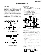
AF Signal System
The detection signal (DEO) from the TX-RX unit goes to
the audio processor (IC504) of the control unit. The signal
passes through a filter in the audio processor to adjust the
gain, and is output to IC502. IC502 sums the AF signal and
the DTMF signal and returns the resulting signal to the TX-
RX unit. The signal (AFO) sent to the TX-RX unit is input to
the D/A converter (IC5). The AFO output level is adjusted by
the D/A converter. The signal output from the D/A converter
is added with the BEEP signal (BPO) and the resulting signal
is input to the audio power amplifier (IC10). The AF signal
from IC10 switches between the internal speaker and
speaker jack (J1) output.
■
Squelch Circuit
The detection output from the FM IF IC (IC11) is ampli-
fied by IC2 and the signal (DEO) is sent to the control unit.
The signal passes through a high-pass filter and a noise am-
plifier (Q503) in the control unit to detect noise. A voltage is
applied to the CPU (IC511). The CPU controls squelch ac-
cording to the voltage (ASQ) level. The signal from the RSSI
pin of IC11 is monitored. The electric field strength of the
receive signal can be known before the ASQ voltage is input
to the CPU, and the scan stop speed is improved.
FIg. 3
AF signal system
IC2
AMP
IC503
AMP
Q503
NOISE AMP D509
IC11
IC511
DEO
RSSI
HPF
DET
CPU
IF
SYSTEM
CONTROL UNIT
Fig. 4
Squelch circuit
IC504
IC3
Q103
IC711
MIC
AF AMP
TA75S01F
MIC KEY
INPUT
AF AMP,
IDC, LPF
TC35453F
IC511
CPU
30620M8
-394GP
SUM AMP
TA75W558FU
X1
VCXO
16.8MHz
VCO
2SK508NV
(K53)
IC300
PLL
SA7025DK
Q106
RF AMP
2SC4215
(Y)
Q300
BUFFER
2SC4215
(Y)
Q203
RF AMP
2SC3357
Q204
ANT
RF AMP
2SC2954
IC400
POWER AMP
M68729
Q7
BUFFER
2SC4215
(Y)
Fig. 5
Transmitter system (K,E type)
CIRCUIT DESCRIPTION
LPF
ANT
L203
BPF
L207
BPF
Q201
AMP
Q15
AMP
IC2
AMP
IC200
MIX
XF1
BPF
D211
D209,210
ANT
SW
+
–
Q203
AMP
CF2
IC11
MIX,IF,DET
X2
2nd
local OSC
1st local
OSC (HT)
DEO
Fig. 2
Receiver system (M type)
Transmitter System
■
Outline
The transmitter circuit produces and amplifies the de-
sired frequency directly. It FM-modulates the carrier signal
by means of a varicap diode.
■
VCO/PLL Circuit
The TK-785 has a VCO for the transmitter and a VCO for
the receiver in a sub-unit (A1). They are housed in a solid
shielded case and connected to the TX-RX unit through
CN101. One of the VCOs is selected with an ST signal. A
filtered low-noise power supply is used for the VCOs and
varicap diodes.
The VCO for the transmitter is described below. It is de-
signed so that Q103 turns on with a prescribed frequency
when a reverse bias is applied to D102 and D107 by using
the control voltage (CV) through CN101. The control voltage
is changed by turning the trimmer capacitor (TC102). The
output from Q103 is applied to the buffer amplifier (Q106) to
generate a VCO output signal. This signal is used as a drive
input signal or a local signal of the first mixer.
AUDIO
PROCE.
SUM
AMP
D/A
CONV.
IC504
IC502
IC5
AF PA
IC10
SP
DTMF
BPO
AFO
DEO
CONTORL UNIT


