TKR-740
27
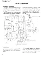
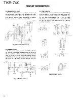
2.3 Transmitter DDS circuit
The transmitter DDS circuit produces the reference
frequency signal (4.5 M Hz) for the transmitter main PLL and
modulates the low -frequency components of digital pager
modulation. This circuit consists of Q241, IC202, IC107, Q207,
Q240, and Q242. The 19.2M Hz signal coming from the
transmitter sub PLL is amplified by Q241 and fed to IC202.
IC202 produces the 4.5M Hz reference frequency signal for
the transmitter main PLL based on the 19.2M Hz signal. Since
the comparison frequency of the transmitter main PLL is 100
kHz, the PLL frequency step is 100 kHz. How ever, fine
CIRCUIT DESCRIPTION
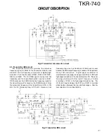
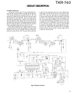
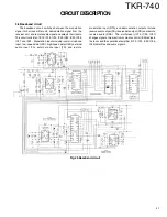
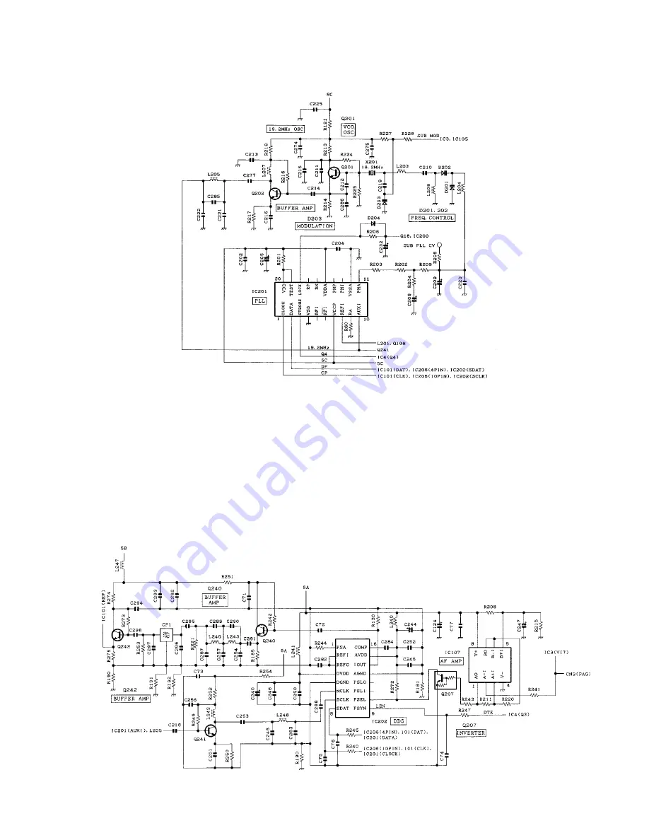
Fig.2 Transmitter reference PLL circuit
frequency steps, such as 2.5kHz and 1.25kHz, can be used
because the DDS output frequency is variable. IC202 performs
binary FSK m odulat ion. Digit al pager m odulat ion is
implemented by applying low -range modulation to DDS and
high-range modulation to the transmitter main PLL. There is a
tw o-stage Butterw orth filter (cutoff frequency: 1.9kHz)
consisting of IC102 in the high-range modulation line. The
IC102 shift input is delayed by IC107 and IC207 to maintain
phase balance betw een the low and high ranges. (See the
level adjustment circuit description.)
Fig.3 Transmitter DDS circuit
Summary of Contents for TKR-740
Page 97: ...TKR 740 TKR 740 BLOCKDIAGRAM 121 122 ...
Page 99: ...TKR 740 TKR 740 INTERCONNECTION DIAGRAM 125 126 ...
Page 101: ...MEMO 129 ...

